 ChipApex | Global Electronic Components Supplier
SEARCH
Search Product
Search Post
— IC芯片 | 连接器 | 传感器 | 被动器件 —
Search productSearch post
— IC芯片 | 连接器 | 传感器 | 被动器件 —
Consult the customer manager about the wholesale price.
consultation hotline:86-132-6715-2157
email:[email protected]
Contact the product manager for consultation. One-stop consultation is available.
Do you want a lower wholesale price? Please send us your inquiry and we will reply immediately.
The Nexperia 74HC05PW,112 is a hex inverter with open-drain outputs housed in a TSSOP14 package (SOT402-1). It operates within a supply voltage range of 2.0 V to 6.0 V and supports an ambient temperature range from -40 °C to +125 °C. The device features CMOS input levels and complies with JEDEC standard no. 7A. Static characteristics include a maximum low-level output voltage of 0.4 V at 4.0 mA drive current (VCC = 4.5 V) and a typical input capacitance of 3.5 pF. Dynamic performance specifies a maximum propagation delay of 27 ns at VCC = 4.5 V and 125 °C.
Verify the specific ordering suffix '112' corresponds to the tube packaging format as defined in the official Nexperia documentation. Confirm that the TSSOP14 package variant matches the required board layout dimensions. Ensure design compliance with the specified operating temperature and voltage limits before finalizing procurement orders.
Select this component when open-drain output capability is required for bus sharing or wired logic implementation. The wide supply voltage range allows flexibility in system power design. Verify that the TSSOP14 package fits the available PCB footprint and that thermal derating requirements are met for the intended operating environment.
This part belongs to the 74HC series of high-speed CMOS logic devices manufactured by Nexperia. The 74HC05 specifically provides six independent inverters with open-drain outputs. The PW suffix indicates the TSSOP14 plastic thin shrink small outline package, while the 112 suffix denotes the specific tube packaging configuration.
Direct replacements include other 74HC05 variants such as 74HC05D,112 (SOIC-14 package) or 74HC05BQ (DHVQFN14 package), provided the package footprint is compatible. Cross-vendor equivalents must match the HC logic family specifications and open-drain output characteristics.
The outputs are open-drain type, meaning they can only pull the signal to ground (LOW). A pull-up resistor is necessary to establish the HIGH logic level when the output transistor is off.
The recommended operating conditions specify a maximum supply voltage (VCC) of 6.0 V.
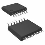 74HC05PW,112
The activity of extra discounts on wholesale prices is in full swing…
Please fill in your contact information and we will send you the latest wholesale price list.





