 ChipApex | Global Electronic Components Supplier
SEARCH
Search Product
Search Post
— IC芯片 | 连接器 | 传感器 | 被动器件 —
Search productSearch post
— IC芯片 | 连接器 | 传感器 | 被动器件 —
Consult the customer manager about the wholesale price.
consultation hotline:86-132-6715-2157
email:[email protected]
Contact the product manager for consultation. One-stop consultation is available.
Do you want a lower wholesale price? Please send us your inquiry and we will reply immediately.
The Nexperia 74HC08PW-Q100/AUJ is a quad 2-input AND gate qualified to AEC-Q100 Grade 1 standards for automotive applications. It operates within a supply voltage range of 2.0 V to 6.0 V and supports ambient temperatures from -40 °C to +125 °C. The device features CMOS low power dissipation, high noise immunity, and latch-up performance exceeding 100 mA per JESD 78 Class II Level B. Inputs include clamp diodes for interfacing with voltages exceeding VCC. ESD protection exceeds 2000 V (HBM) and 1000 V (CDM). Propagation delay is typically 7 ns at 5.0 V with 15 pF load.
Verify the specific ordering suffix against the manufacturer's official documentation to confirm package type and temperature grade. Ensure the component meets AEC-Q100 Grade 1 requirements for your target application. Cross-reference the datasheet revision date to confirm the latest specifications are being utilized during design validation.
Select this component when automotive reliability and wide voltage operation are required. The TSSOP14 package offers space efficiency for surface mount designs. Consider the HC series input levels for CMOS compatibility or HCT variants if TTL level interfacing is necessary. Verify thermal derating requirements for total power dissipation based on the specific ambient conditions.
This part belongs to the Nexperia 74HC08-Q100 family of quad 2-input AND gates. It is designed as a replacement for standard 74HC08 logic in automotive contexts. The PW suffix indicates the TSSOP14 plastic thin shrink small outline package. It complies with JEDEC standards JESD8C and JESD7A for voltage ranges.
Direct pin-compatible replacements within the same family include the 74HC08D-Q100 (SO14 package) and 74HC08BQ-Q100 (DHVQFN14 package). Ensure the substitute maintains the required AEC-Q100 Grade 1 qualification and matches the TSSOP14 footprint if board space is constrained.
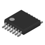 74HC08PW-Q100/AUJ
The activity of extra discounts on wholesale prices is in full swing…
Please fill in your contact information and we will send you the latest wholesale price list.





