 ChipApex | Global Electronic Components Supplier
SEARCH
Search Product
Search Post
— IC芯片 | 连接器 | 传感器 | 被动器件 —
Search productSearch post
— IC芯片 | 连接器 | 传感器 | 被动器件 —
Consult the customer manager about the wholesale price.
consultation hotline:86-132-6715-2157
email:[email protected]
Contact the product manager for consultation. One-stop consultation is available.
Do you want a lower wholesale price? Please send us your inquiry and we will reply immediately.
The 74HC109DB,112 is a dual positive-edge-triggered J-K flip-flop manufactured by Nexperia USA Inc. in the SSOP-16 package. It features individual J and K inputs, clock (CP) inputs, asynchronous active-low set (SD) and reset (RD) inputs, and complementary Q and Q outputs. The device supports a wide supply voltage range of 2.0 V to 6.0 V and operates within a temperature range of -40 °C to +125 °C. It includes Schmitt-trigger action on the clock input for tolerance to slow rise/fall times and provides ESD protection exceeding 2000 V (HBM).
Verify component authenticity through official Nexperia channels due to potential counterfeit risks. Confirm RoHS compliance and specific lot codes against current datasheets. Check for any recent Product Change Notifications (PCN) regarding marking or packaging updates. Ensure design-in compatibility with existing PCB footprints and thermal requirements before finalizing procurement plans.
Select this component when dual edge-triggered memory elements are required in CMOS logic designs. It is suitable for applications needing TTL-compatible input levels if using HCT variants, though HC offers wider voltage ranges. Consider the SSOP-16 package constraints and ensure adequate board space for surface-mount assembly while meeting the specified operating temperature and voltage parameters.
This part belongs to the 74HC series of high-speed CMOS logic devices. It complements other Nexperia logic gates and flip-flops, providing essential sequential logic functionality. The 74HC109 specifically addresses needs for dual J-K configurations, offering flexibility in digital circuit design compared to single-function gates.
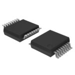 74HC109DB,112
The activity of extra discounts on wholesale prices is in full swing…
Please fill in your contact information and we will send you the latest wholesale price list.






