 ChipApex | Global Electronic Components Supplier
SEARCH
Search Product
Search Post
— IC芯片 | 连接器 | 传感器 | 被动器件 —
Search productSearch post
— IC芯片 | 连接器 | 传感器 | 被动器件 —
Consult the customer manager about the wholesale price.
consultation hotline:86-132-6715-2157
email:[email protected]
Contact the product manager for consultation. One-stop consultation is available.
Do you want a lower wholesale price? Please send us your inquiry and we will reply immediately.
The Nexperia 74HC112D,652 is a dual negative-edge triggered JK flip-flop housed in a 16-pin SO package. It features individual J and K inputs, asynchronous active LOW set (nSD) and reset (nRD) inputs, and complementary nQ and Q outputs. The device operates within a supply voltage range of 2V to 6V and supports an operating temperature range from -40°C to +85°C. Inputs include clamp diodes for interfacing with voltages exceeding VCC.
Verify the specific suffix against official Nexperia documentation to confirm package type and tape/reel specifications. Confirm RoHS compliance status and lead times directly with authorized distributors or the manufacturer. Ensure the selected variant matches the required operating temperature range and ESD protection levels for the target application environment.
Select this component when dual JK functionality with asynchronous control is required. The Schmitt-triggered clock input provides robustness against signal noise. Verify that the 2V to 6V supply range aligns with the system power rails. Consider the 16-pin SO package dimensions for PCB layout constraints compared to alternative packages like TSSOP.
This part belongs to the Nexperia 74HC series of high-speed CMOS logic devices. It implements standard JEDEC-compliant JK flip-flop functionality. The device is designed for general-purpose digital applications requiring reliable state retention and synchronous data transfer triggered by clock edges.
Check for equivalent parts such as the 74HCT112 variant if TTL-level input compatibility is needed instead of CMOS levels. Verify pinout and electrical characteristics match before substitution.
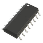 74HC112D,652
The activity of extra discounts on wholesale prices is in full swing…
Please fill in your contact information and we will send you the latest wholesale price list.






