 ChipApex | Global Electronic Components Supplier
SEARCH
Search Product
Search Post
— IC芯片 | 连接器 | 传感器 | 被动器件 —
Search productSearch post
— IC芯片 | 连接器 | 传感器 | 被动器件 —
Consult the customer manager about the wholesale price.
consultation hotline:86-132-6715-2157
email:[email protected]
Contact the product manager for consultation. One-stop consultation is available.
Do you want a lower wholesale price? Please send us your inquiry and we will reply immediately.
The Nexperia 74HC125D/AUJ is a quad buffer and line driver featuring three-state outputs controlled by active-low output enable inputs. It operates within a supply voltage range of 2.0 V to 6.0 V, ensuring CMOS low power dissipation and high noise immunity. The device complies with JEDEC standards JESD8C and JESD7A, supporting input levels compatible with both CMOS and TTL logic families. It includes input clamp diodes for interfacing with voltages exceeding VCC and offers robust ESD protection against human body model and charged device model events.
Verify the specific ordering suffix 'AUJ' against official Nexperia documentation to confirm package type and temperature range specifications. Ensure compatibility with SOIC-14 or TSSOP-14 requirements as defined in the datasheet. Confirm that the procurement channel provides authentic Nexperia products to guarantee adherence to specified electrical characteristics and reliability standards.
Select this component when designing circuits requiring four buffered outputs with independent three-state control. Consider the 2.0 V to 6.0 V operating range for flexibility across different logic voltage domains. Evaluate the high noise immunity and ESD protection features for environments susceptible to electrical interference or static discharge events during operation.
This part belongs to the 74HC/HCT125 family of quad buffers manufactured by Nexperia. It serves as a standard logic interface component for digital systems. The device integrates four independent buffers, each with its own output enable control, facilitating complex bus architectures and signal routing applications in consumer electronics and industrial equipment.
Compatible substitutes include the 74HCT125D for TTL-compatible input levels and other manufacturers' equivalents such as the SN74HC125N. Verify pinout compatibility and electrical parameter alignment before substitution.
A HIGH level on the nOE input forces all outputs into a high-impedance OFF-state, effectively disconnecting them from the circuit.
The input clamp diodes enable the use of current-limiting resistors to safely interface inputs to voltages that exceed the VCC supply voltage.
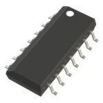 74HC125D/AUJ
The activity of extra discounts on wholesale prices is in full swing…
Please fill in your contact information and we will send you the latest wholesale price list.





