 ChipApex | Global Electronic Components Supplier
SEARCH
Search Product
Search Post
— IC芯片 | 连接器 | 传感器 | 被动器件 —
Search productSearch post
— IC芯片 | 连接器 | 传感器 | 被动器件 —
Consult the customer manager about the wholesale price.
consultation hotline:86-132-6715-2157
email:[email protected]
Contact the product manager for consultation. One-stop consultation is available.
Do you want a lower wholesale price? Please send us your inquiry and we will reply immediately.
The 74HC125D-Q100J is a quad buffer and line driver featuring three-state outputs, manufactured by Nexperia. It operates within a supply voltage range of 2.0 V to 6.0 V and complies with JEDEC standards JESD8C and JESD7A. The device utilizes CMOS technology for low power dissipation and high noise immunity. It includes input clamp diodes to support interfacing with voltages exceeding VCC. Qualified under AEC-Q100 Grade 1, it supports automotive applications across temperature ranges from -40 °C to +85 °C and up to +125 °C.
Verify the specific package variant against the ordering information table. The 'D' suffix indicates an SO14 plastic small outline package (SOT108-1). Confirm that the required temperature grade aligns with the specified -40 °C to +125 °C range. Ensure design compatibility with the active LOW output enable logic before finalizing procurement.
Select this component when a quad buffer with three-state control is required for automotive or industrial environments. The HC series offers CMOS input levels suitable for standard logic families. Consider the SO14 package dimensions if board space allows. Verify that the operating voltage falls within the 2.0 V to 6.0 V range for optimal performance and compliance with JEDEC standards.
This part belongs to the Nexperia 74HCS125/74HC125/74HCT125-Q100 family of quad buffers. The 'HC' designation specifies CMOS input levels, distinguishing it from the 'HCT' variant which uses TTL levels. The 'Q100' suffix denotes automotive qualification. The 'D' package code identifies the SO14 form factor, providing 14 leads in a small outline configuration.
The 74HCT125D-Q100J serves as a functional replacement if TTL input levels are acceptable. Other packages such as TSSOP14 (PW) offer pin-compatible alternatives for different footprint requirements. Verify that any substitute maintains the same AEC-Q100 Grade 1 qualification and three-state output characteristics.
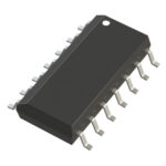 74HC125D-Q100J
The activity of extra discounts on wholesale prices is in full swing…
Please fill in your contact information and we will send you the latest wholesale price list.





