 ChipApex | Global Electronic Components Supplier
SEARCH
Search Product
Search Post
— IC芯片 | 连接器 | 传感器 | 被动器件 —
Search productSearch post
— IC芯片 | 连接器 | 传感器 | 被动器件 —
Consult the customer manager about the wholesale price.
consultation hotline:86-132-6715-2157
email:[email protected]
Contact the product manager for consultation. One-stop consultation is available.
Do you want a lower wholesale price? Please send us your inquiry and we will reply immediately.
The Nexperia 74HC125D,652 is a quad buffer and line driver featuring three-state outputs controlled by active LOW enable inputs. It operates within a supply voltage range of 2.0 V to 6.0 V and supports an ambient temperature range from -40 °C to +125 °C. The device utilizes CMOS technology for low power dissipation and high noise immunity. It complies with JEDEC standards JESD8C and JESD7A. The component is housed in a 14-lead SO plastic small outline package (SOT108-1) with a body width of 3.9 mm.
Verify the specific ordering suffix against official Nexperia documentation to confirm the exact package variant and tape-and-reel specifications. Ensure that the procurement channel provides valid traceability for the SOT108-1 package type. Confirm compliance with RoHS directives as specified in the product data sheet before finalizing acquisition.
Select this component when designing circuits requiring isolated signal transmission or bus holding capabilities. The wide supply voltage range accommodates various system architectures. Verify that the required propagation delay characteristics align with the target clock frequencies and load capacitance conditions defined in the dynamic specifications.
This device belongs to the 74HC/HCT logic family, which represents standard high-speed CMOS technology compatible with Low-power Schottky TTL systems. The 74HC125 variant specifically addresses applications needing buffered outputs with controllable impedance states, distinguishing it from standard non-three-state buffers within the same series.
The 74HCT125D,652 serves as a functional alternative if TTL-compatible input levels are required instead of CMOS levels. Other packages such as TSSOP14 may be considered if board space constraints necessitate a smaller footprint, provided pin compatibility is maintained.
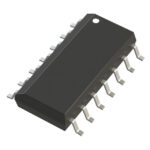 74HC125D,652
The activity of extra discounts on wholesale prices is in full swing…
Please fill in your contact information and we will send you the latest wholesale price list.





