 ChipApex | Global Electronic Components Supplier
SEARCH
Search Product
Search Post
— IC芯片 | 连接器 | 传感器 | 被动器件 —
Search productSearch post
— IC芯片 | 连接器 | 传感器 | 被动器件 —
Consult the customer manager about the wholesale price.
consultation hotline:86-132-6715-2157
email:[email protected]
Contact the product manager for consultation. One-stop consultation is available.
Do you want a lower wholesale price? Please send us your inquiry and we will reply immediately.
The Nexperia 74HC125DB,118 is a quad buffer and line driver featuring four non-inverting buffers with three-state outputs. It operates within a supply voltage range of 2.0 V to 6.0 V and supports an ambient temperature range from -40 °C to +125 °C. The device utilizes CMOS technology for low power dissipation and high noise immunity. Outputs are controlled by active LOW enable inputs (nOE), which force the outputs into a high-impedance OFF-state when HIGH. Inputs include clamp diodes to interface with voltages exceeding VCC.
Verify the package type matches the SO14 plastic small outline package (SOT108-1) specification. Confirm the ordering suffix ,118 corresponds to the standard reel packaging format. Ensure the design accounts for the specified operating temperature range of -40 °C to +125 °C. Check for any specific RoHS compliance requirements relevant to the target market regulations.
Select this component for applications requiring four independent non-inverting buffers with tri-state control. The wide supply voltage range allows compatibility with various logic families. Consider the input clamp diodes for interfacing with higher voltage signals without external protection resistors. Verify that the required propagation delay and output drive current meet the system timing and load requirements.
This part belongs to the 74HC/HCT logic family, designed as a high-speed silicon-gate CMOS device. It is pin-compatible with Low-power Schottky TTL (LSTTL) standards. The device complies with JEDEC standards JESD8C and JESD7A. It provides robust ESD protection exceeding 2000 V according to ANSI/ESDA/JEDEC JS-001 class 2.
Direct replacements include other manufacturers' 74HC125 variants in SOIC-14 packages. Cross-reference with 74HCT125 if TTL input levels are required instead of CMOS levels. Ensure the substitute maintains the same three-state output functionality and active LOW enable control scheme.
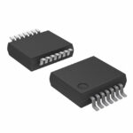 74HC125DB,118
The activity of extra discounts on wholesale prices is in full swing…
Please fill in your contact information and we will send you the latest wholesale price list.





