 ChipApex | Global Electronic Components Supplier

SEARCH
Search Product
Search Post
— IC芯片 | 连接器 | 传感器 | 被动器件 —
Search productSearch post
— IC芯片 | 连接器 | 传感器 | 被动器件 —
Consult the customer manager about the wholesale price.
consultation hotline:86-132-6715-2157
email:[email protected]
Contact the product manager for consultation. One-stop consultation is available.
Do you want a lower wholesale price? Please send us your inquiry and we will reply immediately.
The Nexperia 74HC1GU04GW-Q100,1 is a single unbuffered inverter qualified to AEC-Q100 Grade 1 standards. It operates within a supply voltage range of 2.0 V to 6.0 V and supports ambient temperatures from -40 °C to +125 °C. The device features high noise immunity, symmetrical output impedance, and balanced propagation delays. Static characteristics include an input leakage current maximum of 1.0 μA at 6.0 V and a supply current maximum of 20 μA at 6.0 V. Dynamic performance specifies a propagation delay of up to 90 ns at 2.0 V with 50 pF load, or 18 ns at 4.5 V. Power dissipation capacitance is typically 14 pF.
Verify the specific ordering suffix ',1' corresponds to the required tape and reel packaging configuration. Confirm that the TSSOP5 (SOT353-1) package variant matches the PCB footprint requirements. Ensure the design accounts for the specified power dissipation derating curves above 74 °C to maintain thermal integrity during operation.
Select this component when a single-channel inverter with automotive-grade reliability is required. The wide supply voltage range allows compatibility with both 3.3 V and 5 V logic systems. Consider the unbuffered nature of the gate for applications requiring specific drive characteristics or linear operation modes rather than standard digital switching.
This part belongs to the Nexperia 74HC1GU04-Q100 family of single unbuffered inverters. It shares functional similarities with other AEC-Q100 qualified logic gates but is distinct in its single-inverter topology. The 'GW' designation identifies the TSSOP5 plastic thin shrink small outline package, while the 'Q100' suffix indicates automotive qualification status.
Direct substitutes include the 74HC1GU04GV-Q100, which utilizes the SC-74A (SOT753) package instead of TSSOP5. Other family members like the 74HC1G14GW-Q100 offer Schmitt-trigger inputs but differ functionally. Verify pinout compatibility and package dimensions before substituting.
Yes, the inputs include clamp diodes, allowing them to be driven by voltages exceeding VCC when used with current-limiting resistors.
The recommended operating condition specifies a maximum supply voltage (VCC) of 6.0 V.
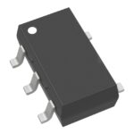 74HC1GU04GW-Q100,1

The activity of extra discounts on wholesale prices is in full swing…
Please fill in your contact information and we will send you the latest wholesale price list.





