 ChipApex | Global Electronic Components Supplier

SEARCH
Search Product
Search Post
— IC芯片 | 连接器 | 传感器 | 被动器件 —
Search productSearch post
— IC芯片 | 连接器 | 传感器 | 被动器件 —
Consult the customer manager about the wholesale price.
consultation hotline:86-132-6715-2157
email:[email protected]
Contact the product manager for consultation. One-stop consultation is available.
Do you want a lower wholesale price? Please send us your inquiry and we will reply immediately.
74HC237PWJ is listed in the Signal Switches, Multiplexers, Decoders range at ChipApex. The manufacturer field lists Nexperia USA Inc.. Its product description is IC DECODER/DEMUX 1X3:8 16TSSOP. Review the specifications below when checking this part for your BOM.
The Nexperia 74HC237PWJ is a 3-to-8 line decoder and demultiplexer featuring address latches, manufactured in a TSSOP16 package (SOT403-1). It operates on a single supply voltage ranging from 2.0 V to 6.0 V. The device decodes three binary weighted address inputs to eight mutually exclusive active HIGH outputs. Key electrical parameters include a propagation delay of up to 48 ns at 6.0 V, an operating temperature range of -40 °C to +125 °C, and ESD protection exceeding 2000 V (HBM) and 1000 V (CDM).
Verify the specific suffix 'J' against official Nexperia documentation to confirm packaging details such as reel specifications or tape dimensions. Ensure the ordered component matches the TSSOP16 form factor and that the manufacturer source aligns with the provided datasheet revision. Confirm RoHS compliance status through the manufacturer's current product change notifications.
Select this component when address latching functionality is required within a decoder circuit. The wide supply voltage range supports various logic families. Verify that the output drive requirements and noise immunity levels meet the system design constraints. Consider the thermal derating characteristics if operating near maximum power dissipation limits.
This part belongs to the 74HC series of high-speed CMOS logic devices. It serves as a specialized variant of standard decoders by incorporating internal latches at the address inputs. This integration reduces external component count in designs requiring stable address selection during data transfer operations.
The 74HC237D is a documented alternative in the SO16 package. Verify pin compatibility and package dimensions before substitution. Ensure the replacement part meets the same electrical specifications and environmental ratings required by the application.
When the latch enable (LE) is LOW, the decoder responds directly to address inputs. When LE transitions HIGH, the last address state is stored, and subsequent address changes are ignored until LE goes LOW again.
E1 (active LOW) and E2 (active HIGH) control the output state independently of the address inputs. All outputs remain HIGH unless E1 is LOW and E2 is HIGH.
Explore related parts through Logic, Integrated Circuits (ICs), all product categories, ChipApex homepage.
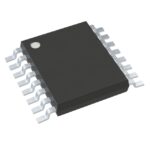 74HC237PWJ

The activity of extra discounts on wholesale prices is in full swing…
Please fill in your contact information and we will send you the latest wholesale price list.





