 ChipApex | Global Electronic Components Supplier
74HC367D,653
Search Product
Search Post
— IC芯片 | 连接器 | 传感器 | 被动器件 —
Search productSearch post
— IC芯片 | 连接器 | 传感器 | 被动器件 —
Consult the customer manager about the wholesale price.
consultation hotline:86-132-6715-2157
email:[email protected]
Contact the product manager for consultation. One-stop consultation is available.
Do you want a lower wholesale price? Please send us your inquiry and we will reply immediately.
The Nexperia 74HC367D,653 is a hex buffer and line driver featuring three-state outputs controlled by active-low output enable inputs (nOE). It operates within a supply voltage range of 2.0 V to 6.0 V and utilizes CMOS technology for low power dissipation. The device includes input clamp diodes to facilitate interfacing with voltages exceeding VCC. Packaged in an SO16 plastic small outline package (SOT109-1), it supports an operating temperature range from -40 °C to +125 °C.
Verify the specific ordering suffix matches the required package type, as the 74HC367 series is available in both SO16 and TSSOP16 variants. Confirm that the selected component aligns with the intended operating temperature range and supply voltage requirements for your specific application design constraints.
Select this component when designing systems requiring non-inverting buffering with controllable bus isolation. The wide supply voltage range accommodates various logic families, while the three-state capability prevents bus contention in multi-driver environments. Ensure the load capacitance remains within specified limits to maintain acceptable propagation delay characteristics.
This part belongs to the 74HC logic family, which provides standard CMOS functionality with high-speed operation. The 74HC367 specifically addresses applications needing multiple buffered outputs with tri-state control. It serves as a fundamental building block for digital interface circuits where signal integrity and bus management are critical design parameters.
Direct functional equivalents include the 74HCT367D,653 for TTL-compatible input levels. Other manufacturers may offer pin-compatible alternatives such as SN74HC367 or MC74HC367, but verify electrical specifications and package dimensions before substitution.
When the nOE input is HIGH, the outputs assume a high impedance OFF-state, effectively disconnecting them from the bus. When nOE is LOW, the buffers transmit the input signals to the outputs.
The input clamp diodes allow the use of current-limiting resistors to interface the inputs to voltages in excess of VCC without damaging the device.
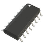 74HC367D,653
The activity of extra discounts on wholesale prices is in full swing…
Please fill in your contact information and we will send you the latest wholesale price list.





