 ChipApex | Global Electronic Components Supplier
SEARCH
Search Product
Search Post
— IC芯片 | 连接器 | 传感器 | 被动器件 —
Search productSearch post
— IC芯片 | 连接器 | 传感器 | 被动器件 —
Consult the customer manager about the wholesale price.
consultation hotline:86-132-6715-2157
email:[email protected]
Contact the product manager for consultation. One-stop consultation is available.
Do you want a lower wholesale price? Please send us your inquiry and we will reply immediately.
The NXP USA Inc. 74HC4052PW/AUJ is a dual single-pole quad-throw analog switch (2 × SP4T) housed in a TSSOP16 package (SOT403-1). It functions as a dual 4-channel analog multiplexer/demultiplexer with independent inputs/outputs (nY0–nY3) and common terminals (nZ). The device operates on a VCC supply of 2.0 V to 10.0 V, supporting an analog input range from -5 V to +5 V. Key electrical parameters include a typical ON resistance of 80 Ω at VCC - VEE = 4.5 V, propagation delay of 15 ns max at VCC = 4.5 V, and ESD protection exceeding 2000 V (HBM).
Verify the specific ordering suffix against the manufacturer's current product data sheet to confirm package type and temperature range specifications. Ensure the component source matches the authorized Nexperia or NXP distribution channels to guarantee authenticity and compliance with JEDEC standards.
Select this component when a dual 4:1 analog switch configuration is required within a 16-pin surface-mount footprint. Confirm that the system supply voltage falls within the 2.0 V to 10.0 V range and that the analog signals remain between -5 V and +5 V. Verify thermal dissipation requirements against the TSSOP16 package derating curves.
This part belongs to the 74HC/HCT4052 family of high-speed Si-gate CMOS devices. It maintains pin compatibility with the legacy 4000B series while offering improved performance characteristics. The PW suffix specifically denotes the plastic thin shrink small outline package variant manufactured by Nexperia.
Direct functional substitutes include the 74HCT4052PW for TTL-compatible logic levels. Other packages such as SO16 (74HC4052D) or DHVQFN16 (74HC4052BQ) offer identical functionality with different mechanical footprints.
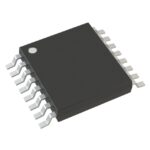 74HC4052PW/AUJ
The activity of extra discounts on wholesale prices is in full swing…
Please fill in your contact information and we will send you the latest wholesale price list.





