 ChipApex | Global Electronic Components Supplier
SEARCH
Search Product
Search Post
— IC芯片 | 连接器 | 传感器 | 被动器件 —
Search productSearch post
— IC芯片 | 连接器 | 传感器 | 被动器件 —
Consult the customer manager about the wholesale price.
consultation hotline:86-132-6715-2157
email:[email protected]
Contact the product manager for consultation. One-stop consultation is available.
Do you want a lower wholesale price? Please send us your inquiry and we will reply immediately.
The Nexperia 74HC4067BQ-Q100J is an automotive-qualified single-pole 16-throw analog switch (SP16T) housed in a DHVQFN24 package. It operates on a supply voltage range of 2.0 V to 10.0 V with a maximum power dissipation of 500 mW. The device features four digital select inputs and one active-low enable input, controlling sixteen independent I/O channels. Key electrical parameters include a typical ON resistance of 80 Ω at 4.5 V, propagation delay up to 19 ns at 4.5 V, and turn-off time up to 63 ns. It supports an operating temperature range from -40 °C to +125 °C.
Verify that the specific suffix BQ corresponds to the DHVQFN24 package variant required for your layout. Confirm the Q100 designation matches your automotive grade requirements. Ensure the ordering code includes the correct tape and reel specifications if applicable. Cross-reference the manufacturer part number against official Nexperia documentation to validate authenticity.
Select this component when a 16-channel analog switch is needed within an automotive context requiring AEC-Q100 compliance. The HC logic family allows operation across a wide voltage spectrum from 2.0 V to 10.0 V. Verify that the DHVQFN24 footprint fits your PCB constraints and that the thermal performance meets your system's dissipation needs.
This device belongs to the 74HC4067-Q100 series, which represents the high-speed CMOS version of the standard 4067 multiplexer. The 'BQ' suffix specifically identifies the DHVQFN24 package type, while 'Q100' indicates automotive qualification. It serves as the HC equivalent to the 74HCT4067-Q100, differing primarily in input logic voltage thresholds.
The 74HC4067PW-Q100 offers identical electrical functionality but utilizes a TSSOP24 package instead of DHVQFN24. Designers must verify pin compatibility and physical footprint differences before substituting packages within the same functional family.
The enable input (E) is active LOW. When E is HIGH, all switches are turned off regardless of the state of the address inputs S0 through S3.
The inputs include clamp diodes that enable the use of current-limiting resistors to interface inputs to voltages in excess of VCC without damaging the device.
Yes, the device features built-in 'break before make' logic to prevent momentary shorts between channels during switching operations.
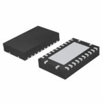 74HC4067BQ-Q100J
The activity of extra discounts on wholesale prices is in full swing…
Please fill in your contact information and we will send you the latest wholesale price list.





