 ChipApex | Global Electronic Components Supplier

SEARCH
Search Product
Search Post
— IC芯片 | 连接器 | 传感器 | 被动器件 —
Search productSearch post
— IC芯片 | 连接器 | 传感器 | 被动器件 —
Consult the customer manager about the wholesale price.
consultation hotline:86-132-6715-2157
email:[email protected]
Contact the product manager for consultation. One-stop consultation is available.
Do you want a lower wholesale price? Please send us your inquiry and we will reply immediately.
The Nexperia 74HC4075PW-Q100J is a triple 3-input OR gate housed in a TSSOP14 (SOT402-1) package. It complies with JEDEC JESD7A standards and features input clamp diodes for interfacing with voltages exceeding VCC. The device operates within a supply voltage range of 2.0 V to 6.0 V, supporting CMOS input levels. It is qualified to AEC-Q100 Grade 1 standards, ensuring suitability for automotive applications across specified temperature ranges.
Verify the specific suffix 'J' against official Nexperia documentation to confirm tape and reel packaging specifications. Ensure the design accounts for the TSSOP14 thermal derating characteristics above 81 °C. Confirm that the application environment strictly adheres to the AEC-Q100 Grade 1 qualification requirements defined in the datasheet.
Select this component when a triple 3-input OR function is required in an automotive-grade environment. The HC series offers wide supply voltage flexibility compared to HCT variants. Verify that the TSSOP14 package dimensions align with the PCB footprint constraints and that the CMOS input thresholds match the driving source logic levels.
This part belongs to the Nexperia 74HC_HCT4075_Q100 family of triple 3-input OR gates. The PW suffix indicates the TSSOP14 plastic thin shrink small outline package. The Q100 designation confirms its automotive qualification status, distinguishing it from standard commercial grade counterparts while maintaining functional compatibility with the broader 74HC logic family.
Direct substitutes include the 74HC4075D-Q100 in an SO14 package. Cross-family replacements like the 74HCS4075PW-Q100J offer similar functionality but may differ in drive strength and speed characteristics. Always verify pinout compatibility and electrical parameters before substitution.
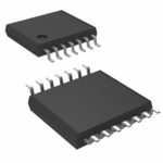 74HC4075PW-Q100J

The activity of extra discounts on wholesale prices is in full swing…
Please fill in your contact information and we will send you the latest wholesale price list.





