 ChipApex | Global Electronic Components Supplier
SEARCH
Search Product
Search Post
— IC芯片 | 连接器 | 传感器 | 被动器件 —
Search productSearch post
— IC芯片 | 连接器 | 传感器 | 被动器件 —
Consult the customer manager about the wholesale price.
consultation hotline:86-132-6715-2157
email:[email protected]
Contact the product manager for consultation. One-stop consultation is available.
Do you want a lower wholesale price? Please send us your inquiry and we will reply immediately.
The Nexperia 74HC4351DB,112 is an 8-channel analog multiplexer/demultiplexer with address latches in a SO20 (SOT163-1) package. It operates as a single-pole octal-throw switch with three digital select inputs (S0-S2), eight independent I/Os (Yn), and one common I/O (Z). The device supports dual supplies: VCC ranges from 2.0 V to 10.0 V for HC logic, while HCT logic requires 4.5 V to 5.5 V. Analog signals span -5 V to +5 V. Key electrical parameters include a typical ON resistance of 80 Ω at 4.5 V supply and propagation delays up to 15 ns. ESD protection exceeds 2 kV (HBM) and 1 kV (CDM).
Verify the ordering suffix
Select the 74HC variant for wide voltage operation (2.0 V to 10.0 V) and CMOS input levels. Choose the 74HCT variant if TTL-compatible input thresholds are required within a strict 4.5 V to 5.5 V supply range. Ensure the SO20 package fits the PCB layout constraints compared to alternative packages like TSSOP20.
This component belongs to the standard 74HC/HCT logic family manufactured by Nexperia. It is functionally compatible with other manufacturers' 74HC4351 devices adhering to JEDEC standard no. 7A. The part serves as a general-purpose analog switch suitable for both digital and low-frequency analog signal routing.
Direct substitutes include the 74HC4351D and 74HCT4351D from Nexperia. Cross-brand equivalents such as the CD4051 or MC14051 offer similar functionality but may differ in speed and drive capability. Verify pinout compatibility and voltage ratings when substituting.
When LE is HIGH, the latch is transparent, allowing changes in S0-S2 to immediately update the selected channel. When LE goes LOW, the last state of the select inputs is stored, maintaining the current channel selection regardless of subsequent changes on S0-S2.
All eight switches are turned off (high impedance) when E1 is HIGH or E2 is LOW. Normal operation requires E1 to be LOW and E2 to be HIGH.
Yes, the device supports a wide analog input voltage range from -5 V to +5 V. However, the absolute maximum rating states that voltages at Yn and Z may not exceed VCC or VEE without risking damage, so external clamping or careful biasing is required for signals beyond the supply rails.
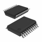 74HC4351DB,112
The activity of extra discounts on wholesale prices is in full swing…
Please fill in your contact information and we will send you the latest wholesale price list.





