 ChipApex | Global Electronic Components Supplier
SEARCH
Search Product
Search Post
— IC芯片 | 连接器 | 传感器 | 被动器件 —
Search productSearch post
— IC芯片 | 连接器 | 传感器 | 被动器件 —
Consult the customer manager about the wholesale price.
consultation hotline:86-132-6715-2157
email:[email protected]
Contact the product manager for consultation. One-stop consultation is available.
Do you want a lower wholesale price? Please send us your inquiry and we will reply immediately.
The Nexperia 74HC4851BQ,115 is an 8-channel analog multiplexer/demultiplexer housed in a DHVQFN16 package (SOT763-1). It operates on a single supply voltage ranging from 4.5 V to 5.5 V and supports an ambient temperature range of -40 °C to +125 °C. The device features three digital select inputs (S0 to S2) and an active-LOW enable input (E). Key electrical parameters include a maximum ON-state resistance of 210 Ω at 4.5 V, propagation delays up to 17 ns, and enable/disable times reaching 100 ns. It provides ESD protection exceeding 2000 V (HBM) and 1000 V (CDM), with latch-up performance meeting JESD 78 Class II standards.
Verify the specific ordering suffix against official Nexperia documentation to confirm the DHVQFN16 package type and lead-free status. Ensure the application environment remains within the specified 4.5 V to 5.5 V supply voltage range and the -40 °C to +125 °C operating temperature limits to maintain guaranteed performance characteristics.
Select this component when a high-density surface-mount solution is required for 8-channel switching. The DHVQFN16 package offers thermal enhancement suitable for compact designs. Confirm that the HCT logic family compatibility aligns with the system's 5 V digital interface requirements before finalizing the design.
This part belongs to the 74HC/HCT4851 series of 8-channel analog multiplexers. It shares functional similarities with other variants like the 74HC4851PW but differs in package geometry and logic threshold levels. The BQ suffix specifically denotes the DHVQFN16 package configuration, distinguishing it from SO or TSSOP alternatives.
Direct pin-compatible replacements include the 74HC4851BQ and 74HCT4851BQ from the same manufacturer. Verify that any substitute maintains the DHVQFN16 footprint and meets the required injection-current cross-coupling specifications.
It allows signals at disabled analog input channels to exceed the supply voltage without affecting the signal of the enabled analog channel, eliminating the need for external diode/resistor networks.
At the minimum recommended supply voltage of 4.5 V, the maximum ON-state resistance is 210 Ω.
Yes, the eight independent inputs/outputs (Y0 to Y7) and the common input/output (Z) allow the device to function as both a multiplexer and a demultiplexer.
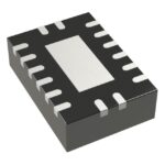 74HC4851BQ,115
The activity of extra discounts on wholesale prices is in full swing…
Please fill in your contact information and we will send you the latest wholesale price list.





