 ChipApex | Global Electronic Components Supplier

SEARCH
Search Product
Search Post
— IC芯片 | 连接器 | 传感器 | 被动器件 —
Search productSearch post
— IC芯片 | 连接器 | 传感器 | 被动器件 —
Consult the customer manager about the wholesale price.
consultation hotline:86-132-6715-2157
email:[email protected]
Contact the product manager for consultation. One-stop consultation is available.
Do you want a lower wholesale price? Please send us your inquiry and we will reply immediately.
74HC75DB,112 is listed in the Latches range at ChipApex. The manufacturer field lists Nexperia USA Inc.. Its product description is IC QUAD BIST TRANSP LATCH 16SSOP. Review the specifications below when checking this part for your BOM.
The Nexperia 74HC75DB,112 is a quad bistable transparent latch housed in a TSSOP16 package (SOT403-1). It operates on a supply voltage range of 2.0 V to 6.0 V and complies with JEDEC standards JESD8C and JESD7A. The device features complementary Q and nQ outputs, with VCC and GND located on center pins. It includes clamp diodes on inputs for overvoltage interfacing. ESD protection exceeds 2000 V (HBM) and 1000 V (CDM). Operating temperatures span from -40 °C to +125 °C.
Verify the specific ordering suffix
Select this component when a quad latch configuration is required within standard CMOS logic families. Ensure the design accommodates the dual enable input structure where latches 1 and 2 share one control line, while latches 3 and 4 share another. Confirm that the TSSOP16 package dimensions align with the PCB footprint requirements and that the operating voltage range matches the system power supply rails.
This part belongs to the Nexperia 74HC series, which utilizes high-speed CMOS technology. The 74HC75 specifically provides four independent bistable latches. Unlike flip-flops triggered by clock edges, these latches are level-sensitive, becoming transparent when the enable input is HIGH and storing data upon the HIGH-to-LOW transition of the enable signal.
Public confirmed substitute: 74HC75PW,118
The four latches are grouped into two pairs. Latches 1 and 2 are controlled by the LE12 input, while latches 3 and 4 are controlled by the LE34 input. Both enable inputs are active HIGH.
When the enable input (LEnn) is LOW, the latched outputs remain stable regardless of changes at the data inputs. The data present at the inputs one setup time prior to the HIGH-to-LOW transition is stored.
Explore related parts through Logic, Integrated Circuits (ICs), all product categories, ChipApex homepage.
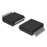 74HC75DB,112

The activity of extra discounts on wholesale prices is in full swing…
Please fill in your contact information and we will send you the latest wholesale price list.





