 ChipApex | Global Electronic Components Supplier
74HCT125PW,112
Search Product
Search Post
— IC芯片 | 连接器 | 传感器 | 被动器件 —
Search productSearch post
— IC芯片 | 连接器 | 传感器 | 被动器件 —
Consult the customer manager about the wholesale price.
consultation hotline:86-132-6715-2157
email:[email protected]
Contact the product manager for consultation. One-stop consultation is available.
Do you want a lower wholesale price? Please send us your inquiry and we will reply immediately.
The Nexperia 74HCT125PW,112 is a quad buffer and line driver featuring three-state outputs controlled by active LOW output enable inputs (nOE). It belongs to the HCT logic family, utilizing TTL input levels for compatibility with standard digital systems. The device operates within a supply voltage range of 4.5 V to 5.5 V. It provides four non-inverting buffers in a TSSOP14 package (SOT402-1), suitable for surface-mount applications across an industrial temperature range of -40 °C to +125 °C.
Verify the specific ordering suffix '112' against official Nexperia documentation to confirm tape-and-reel packaging specifications. Ensure the selected variant matches the required TSSOP14 package dimensions and thermal characteristics for your PCB layout. Cross-reference the full part number with the manufacturer's latest datasheet revision to validate compliance with current environmental directives.
Select this component when designing systems requiring TTL-compatible inputs alongside CMOS drive capabilities. The HCT series ensures low power dissipation while maintaining noise immunity. Consider the TSSOP14 package for space-constrained designs requiring surface-mount technology. Verify that the operating temperature range meets the environmental requirements of the target application.
This component is part of the broader 74HCT125 family, which includes variants in different packages such as SO14. The PW suffix specifically denotes the TSSOP14 plastic thin shrink small outline package. It shares functional equivalence with other quad buffer devices but is distinguished by its specific HCT logic family characteristics and pinout configuration.
Compatible substitutes include the 74HC125PW for CMOS input levels or generic 74HCT125 equivalents from other manufacturers, provided they maintain identical pinouts and electrical specifications. Verify that any replacement device supports the same TSSOP14 package and operates within the specified voltage and temperature ranges.
The outputs assume a high-impedance OFF-state when the nOE input is HIGH. When nOE is LOW, the data from the inputs is transmitted to the outputs.
The input clamp diodes allow the use of current-limiting resistors to interface the inputs to voltages that exceed the supply voltage (VCC).
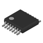 74HCT125PW,112
The activity of extra discounts on wholesale prices is in full swing…
Please fill in your contact information and we will send you the latest wholesale price list.





