 ChipApex | Global Electronic Components Supplier
74HCT1G125GW,125
Search Product
Search Post
— IC芯片 | 连接器 | 传感器 | 被动器件 —
Search productSearch post
— IC芯片 | 连接器 | 传感器 | 被动器件 —
Consult the customer manager about the wholesale price.
consultation hotline:86-132-6715-2157
email:[email protected]
Contact the product manager for consultation. One-stop consultation is available.
Do you want a lower wholesale price? Please send us your inquiry and we will reply immediately.
The Nexperia 74HCT1G125GW,125 is a single non-inverting buffer and line driver featuring three-state outputs. It operates within a supply voltage range of 4.5 V to 5.5 V and accepts TTL-level inputs. The device provides balanced propagation delays and symmetrical output impedance. It is housed in a TSSOP5 plastic thin shrink small outline package (SOT353-1) with five leads and a body width of 1.25 mm. The component supports an ambient operating temperature from -40 °C to +125 °C.
Verify that the specific part number suffix matches the required package type and temperature range. Confirm the logic family designation corresponds to TTL input levels rather than CMOS levels. Ensure the ordering information aligns with the correct product data sheet revision to avoid discrepancies in electrical specifications or marking codes.
Select this component when TTL-compatible input switching levels are required alongside three-state bus control capabilities. The device is suitable for designs needing balanced propagation delays and symmetrical output impedance. Consider the TSSOP5 package dimensions if space constraints exist on the printed circuit board layout.
This component belongs to the 74HCT1G series of single-gate logic devices manufactured by Nexperia. It shares functional similarities with the 74HC1G125 but differs in input voltage thresholds, specifically supporting TTL logic levels. The series is designed for general-purpose buffering and line driving tasks in digital electronic systems.
Direct substitutes include the 74AHCT1G125SE-7, 74AHCT1G125DBVRE4, 74AHCT1G125DBVRG4, and 74AHCT1G125DBVTG4.
The OE pin is the output enable input which is active LOW. When HIGH, it forces the output into a high-impedance OFF-state.
Yes, the inputs include clamp diodes, enabling the use of current limiting resistors to interface with voltages exceeding VCC.
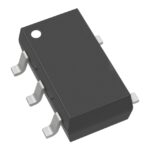 74HCT1G125GW,125
The activity of extra discounts on wholesale prices is in full swing…
Please fill in your contact information and we will send you the latest wholesale price list.





