 ChipApex | Global Electronic Components Supplier

SEARCH
Search Product
Search Post
— IC芯片 | 连接器 | 传感器 | 被动器件 —
Search productSearch post
— IC芯片 | 连接器 | 传感器 | 被动器件 —
Consult the customer manager about the wholesale price.
consultation hotline:86-132-6715-2157
email:[email protected]
Contact the product manager for consultation. One-stop consultation is available.
Do you want a lower wholesale price? Please send us your inquiry and we will reply immediately.
74HCT259D,652 is listed in the Latches range at ChipApex. The manufacturer field lists Nexperia USA Inc.. Its product description is NEXPERIA 74HCT259D - D LATCH, HC. Review the specifications below when checking this part for your BOM.
The Nexperia 74HCT259D,652 is an 8-bit addressable latch in the HCT logic family. It operates within a supply voltage range of 4.5 V to 5.5 V and accepts TTL-level inputs. The device features four modes: addressable latch, memory, demultiplexer, and reset. It utilizes three address inputs (A0-A2) and one data input (D). Outputs are available for each storage bit. The component is housed in a 16-lead SOIC package (SOT109-1) with an operating temperature range from -40 °C to +125 °C.
Verify the specific ordering suffix against the manufacturer's official documentation to confirm the exact package type and temperature rating. Confirm that the required logic family variant matches the application voltage requirements. Check for any recent product change notices or end-of-life announcements directly from the supplier before finalizing procurement plans.
Select this component when TTL-compatible logic levels are required for control signals while maintaining CMOS performance characteristics. Ensure the design accommodates the specified supply voltage limits and thermal dissipation requirements for the SOIC package. Verify that the pinout configuration aligns with the intended PCB layout constraints.
This part belongs to the 74HCT series of integrated circuits manufactured by Nexperia. It is functionally compatible with other devices in the same logic family but offers specific addressing capabilities not found in standard latches or decoders. The D suffix indicates the plastic small outline package variant.
The 74HCT259PW serves as a direct functional substitute utilizing a TSSOP package. Other variants within the 74HCT259 family may be considered if package flexibility is required, provided the electrical specifications remain consistent with the system design.
In memory mode, all latches retain their previous states and remain unaffected by changes to the data or address inputs.
The MR input acts as a conditional reset input. When driven LOW, it forces all outputs to a LOW state regardless of other inputs.
Explore related parts through Logic, Integrated Circuits (ICs), all product categories, ChipApex homepage.
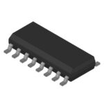 74HCT259D,652

The activity of extra discounts on wholesale prices is in full swing…
Please fill in your contact information and we will send you the latest wholesale price list.





