 ChipApex | Global Electronic Components Supplier
74LCX16652MEA
Search Product
Search Post
— IC芯片 | 连接器 | 传感器 | 被动器件 —
Search productSearch post
— IC芯片 | 连接器 | 传感器 | 被动器件 —
Consult the customer manager about the wholesale price.
consultation hotline:86-132-6715-2157
email:[email protected]
Contact the product manager for consultation. One-stop consultation is available.
Do you want a lower wholesale price? Please send us your inquiry and we will reply immediately.
The 74LCX16652MEA is a low-voltage transceiver and register featuring sixteen non-inverting bidirectional bus transceivers with 3-STATE outputs. It supports multiplexed transmission of data directly from the input bus or from internal registers, clocked by HIGH logic level transitions on CPABn or CPBAn pins. Designed for 2.3V to 3.6V VCC applications, it interfaces with 5V signal environments via 5V tolerant inputs and outputs. Fabricated using advanced CMOS technology, it achieves high-speed operation while maintaining low power dissipation.
Verify that the ordering code matches the specific package type required, as the device is available in both SSOP and TSSOP configurations. Confirm whether tape and reel packaging is needed by checking for the 'X' suffix in the part number. Ensure compatibility with the target system's voltage levels and temperature range specifications before finalizing procurement.
Select this component when designing systems requiring bidirectional data transfer with optional registration capabilities at low voltages. The 5V tolerance feature makes it suitable for bridging different voltage domains without additional level shifters. Consider the propagation delay and output drive current requirements to ensure signal integrity across the bus lines.
This device belongs to the LCX family of low-voltage CMOS logic devices manufactured originally by Fairchild Semiconductor. It serves as a registered bus transceiver designed for high-speed data handling in portable and battery-powered applications where power efficiency and voltage compatibility are critical design constraints.
Check datasheets for equivalent parts from other manufacturers such as NXP or Texas Instruments within the same logic family. Verify pinout compatibility and electrical characteristics like propagation delay and supply voltage ranges to ensure functional interchangeability in existing designs.
Data can be stored in internal D flip-flops upon LOW-to-HIGH clock transitions or transferred in real-time by enabling both Output Enable pins simultaneously, reinforcing the input state on the output bus.
The maximum quiescent supply current (ICC) is specified as 20 µA when the inputs are tied to VCC or GND within the operating voltage range.
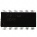 74LCX16652MEA
The activity of extra discounts on wholesale prices is in full swing…
Please fill in your contact information and we will send you the latest wholesale price list.





