ChipApex | Global Electronic Components Supplier

SEARCH
Search Product
Search Post
— IC芯片 | 连接器 | 传感器 | 被动器件 —
Search productSearch post
— IC芯片 | 连接器 | 传感器 | 被动器件 —
Consult the customer manager about the wholesale price.
consultation hotline:86-132-6715-2157
email:[email protected]
Contact the product manager for consultation. One-stop consultation is available.
Do you want a lower wholesale price? Please send us your inquiry and we will reply immediately.
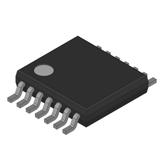
74LV00PW,112 is listed in the Inverter Gates range at ChipApex. The manufacturer field lists Nexperia USA Inc.. Its product description is IC GATE NAND. Review the specifications below when checking this part for your BOM.
The Nexperia USA Inc. 74LV00PW,112 is a quad 2-input NAND gate in the 74LV logic series. It operates within a supply voltage range of 1.0 V to 5.5 V and features CMOS low power dissipation. The device includes input clamp diodes for interfacing with voltages exceeding VCC. It provides latch-up performance exceeding 100 mA per JESD 78 Class II Level B and complies with JEDEC standards for various voltage ranges. ESD protection exceeds 2000 V (HBM) and 1000 V (CDM). The component is specified for operation from -40 °C to +125 °C.
Verify the specific ordering suffix '112' corresponds to the TSSOP14 package (SOT402-1) as defined in the official datasheet. Confirm that the procurement channel sources the exact manufacturer part number to ensure compliance with the stated electrical characteristics and package dimensions. Cross-reference the revision history to ensure the latest product data sheet version is utilized for design integration.
Select this component when a quad 2-input NAND gate is required for low-voltage designs ranging from 1.0 V to 5.5 V. It is suitable for applications needing high noise immunity and compatibility with TTL levels at specific supply voltages. Consider the TSSOP14 package constraints and the specified thermal derating values for total power dissipation above 81 °C during PCB layout planning.
The 74LV00PW,112 belongs to the 74LV family of CMOS logic devices manufactured by Nexperia. This family is optimized for low-voltage applications while maintaining compatibility with standard logic interfaces. The PW suffix indicates the TSSOP14 plastic thin shrink small outline package variant, which offers a compact footprint suitable for space-constrained surface-mount designs.
Public confirmed substitute part numbers include 74LV00D,118.
No, the 74LV00 does not feature I_OFF circuitry for partial power-down mode operation; this feature is specific to other Nexperia families such as the 74AUP.
The maximum input transition rise and fall rate depends on the supply voltage: 50 ns/V for VCC between 3.6 V and 5.5 V, and 100 ns/V for VCC between 2.7 V and 3.6 V.
Explore related parts through Logic, Integrated Circuits (ICs), all product categories, ChipApex homepage.
 74LV00PW,112

The activity of extra discounts on wholesale prices is in full swing…
Please fill in your contact information and we will send you the latest wholesale price list.