 ChipApex | Global Electronic Components Supplier
SEARCH
Search Product
Search Post
— IC芯片 | 连接器 | 传感器 | 被动器件 —
Search productSearch post
— IC芯片 | 连接器 | 传感器 | 被动器件 —
Consult the customer manager about the wholesale price.
consultation hotline:86-132-6715-2157
email:[email protected]
Contact the product manager for consultation. One-stop consultation is available.
Do you want a lower wholesale price? Please send us your inquiry and we will reply immediately.
The Nexperia 74LV164PW,112 is an 8-bit serial-in/parallel-out shift register in a TSSOP14 package. It operates with a supply voltage range of 1.0 V to 5.5 V and features two gated serial data inputs (DSA, DSB) and eight parallel outputs (Q0-Q7). Data shifts on the LOW-to-HIGH clock transition, while an asynchronous master reset clears all outputs. The device complies with JEDEC standards for voltages from 1.65 V to 5.5 V and supports operating temperatures from -40 °C to +125 °C.
Verify the specific ordering suffix '112' corresponds to the TSSOP14 (SOT402-1) package variant when sourcing. Confirm the required temperature grade (-40 °C to +125 °C) matches the application environment. Ensure design compliance with the absolute maximum ratings for supply voltage and clamping currents to prevent device damage during operation.
Select this component for applications requiring low-power CMOS performance across a wide voltage range. It is suitable for systems needing direct TTL level compatibility between 2.7 V and 3.6 V. Consider the TSSOP14 package for space-constrained surface-mount designs requiring thin profile integration.
This part belongs to the 74LV series of low-voltage CMOS logic devices manufactured by Nexperia. The 74LV164 specifically implements an 8-bit shift register function. The PW suffix denotes the plastic thin shrink small outline package with 14 leads, distinguishing it from SO or DHVQFN variants within the same logical family.
Direct pin-compatible alternatives include the 74LV164D (SO14 package) and 74LV164BQ (DHVQFN14 package), provided the physical footprint requirements align with the respective package outlines SOT108-1 and SOT762-1.
A LOW signal on the master reset (MR) input asynchronously clears the register, forcing all outputs (Q0 to Q7) LOW immediately, independent of the clock or data inputs.
Yes, the inputs include clamp diodes which allow the use of current limiting resistors to interface the inputs to voltages in excess of VCC.
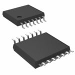 74LV164PW,112
The activity of extra discounts on wholesale prices is in full swing…
Please fill in your contact information and we will send you the latest wholesale price list.





