 ChipApex | Global Electronic Components Supplier

SEARCH
Search Product
Search Post
— IC芯片 | 连接器 | 传感器 | 被动器件 —
Search productSearch post
— IC芯片 | 连接器 | 传感器 | 被动器件 —
Consult the customer manager about the wholesale price.
consultation hotline:86-132-6715-2157
email:[email protected]
Contact the product manager for consultation. One-stop consultation is available.
Do you want a lower wholesale price? Please send us your inquiry and we will reply immediately.
74LV1T08GW-Q100H is listed in the Inverter Gates range at ChipApex. The manufacturer field lists Nexperia USA Inc.. Its product description is 74LV1T08GW-Q100/SOT353/UMT5. Review the specifications below when checking this part for your BOM.
The Nexperia 74LV1T08GW-Q100H is a single, level translating 2-input AND gate qualified to AEC-Q100 Grade 1. It operates on a single supply voltage ranging from 1.6 V to 5.5 V. The device supports up translation (e.g., 1.8 V to 3.3 V) and down translation (e.g., 3.3 V to 1.8 V). It features 5 V tolerant inputs and outputs referenced to the supply voltage. Propagation delay ranges from 3.6 ns to 11.7 ns depending on load capacitance and supply voltage.
Verify the specific suffix 'H' against the official datasheet to confirm package or tape-and-reel variations. Ensure the component meets AEC-Q100 Grade 1 requirements for your target automotive environment. Cross-reference the SOT353-1 package dimensions with your PCB footprint design guidelines before finalizing procurement.
Select this component when a single-supply translator is required for bidirectional level shifting between 1.8 V, 2.5 V, 3.3 V, and 5.0 V domains. It is suitable for mixed-voltage environments where 5 V tolerance is necessary. Consider the propagation delay characteristics relative to your system clock speeds and load capacitance requirements.
This part belongs to the 74LV1T08-Q100 family of translating AND gates. It is designed for automotive applications requiring robust performance across wide temperature ranges. The device integrates level translation logic within a compact TSSOP5 package, facilitating space-constrained designs in modern electronic systems.
Check for direct equivalents within the 74LV1T08-Q100 series that may share identical pinouts and electrical characteristics. Verify if alternative packages like X2SON are functionally interchangeable for your specific application constraints.
The maximum recommended operating supply voltage (VCC) is 5.5 V.
Yes, the I_OFF circuitry disables the output to prevent damaging backflow current when the device is powered down.
Explore related parts through Logic, Integrated Circuits (ICs), all product categories, ChipApex homepage.
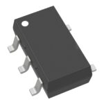 74LV1T08GW-Q100H

The activity of extra discounts on wholesale prices is in full swing…
Please fill in your contact information and we will send you the latest wholesale price list.




