 ChipApex | Global Electronic Components Supplier
74LV1T125GW-Q100H
Search Product
Search Post
— IC芯片 | 连接器 | 传感器 | 被动器件 —
Search productSearch post
— IC芯片 | 连接器 | 传感器 | 被动器件 —
Consult the customer manager about the wholesale price.
consultation hotline:86-132-6715-2157
email:[email protected]
Contact the product manager for consultation. One-stop consultation is available.
Do you want a lower wholesale price? Please send us your inquiry and we will reply immediately.
The Nexperia 74LV1T125GW-Q100H is a single supply translating buffer and line driver featuring a 3-state output, housed in a TSSOP5 (SOT353-1) package. It supports a supply voltage range of 1.6 V to 5.5 V with 5 V tolerant inputs. The device facilitates level translation between 1.8 V, 2.5 V, 3.3 V, and 5.0 V CMOS levels. Propagation delay ranges from 3.2 ns to 11.6 ns depending on load capacitance and voltage. It operates within an ambient temperature range of -40 °C to +125 °C and meets AEC-Q100 Grade 1 qualification standards for automotive applications.
Verify the specific suffix 'Q100H' against official Nexperia documentation to confirm it denotes the standard tape-and-reel packaging format rather than a variant with different electrical characteristics. Ensure the ordering code matches the required SOT353-1 package type. Confirm compliance requirements such as RoHS status directly with the manufacturer's current product data sheet before finalizing procurement specifications.
Select this component when interfacing circuits operating at different voltage levels, specifically requiring translation between 1.8 V and 5.0 V domains. The wide supply voltage range accommodates various system power rails. Consider the 3-state capability if bus sharing or tri-state control is necessary. Verify that the propagation delay and drive strength meet the timing requirements of the target application interface.
This part belongs to the 74LV1T125-Q100 family of single-supply translating buffers. It shares functional similarities with other level translators but is distinguished by its specific 5 V tolerance and single-channel configuration. The Q100 designation indicates automotive-grade qualification, while the GW suffix specifies the thin shrink small outline plastic package.
Check for direct equivalents within the 74LV1T125 series from Nexperia or cross-reference with other manufacturers offering single-supply translating buffers with 3-state outputs. Ensure any substitute maintains the same AEC-Q100 Grade 1 qualification and compatible pinout for the SOT353-1 package.
Yes, the device supports up translation, such as converting 1.8 V input signals to 3.3 V outputs when powered by a 3.3 V supply.
The OE (Output Enable) pin controls the 3-state output. A HIGH level at OE causes the output to assume a high-impedance OFF-state.
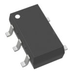 74LV1T125GW-Q100H
The activity of extra discounts on wholesale prices is in full swing…
Please fill in your contact information and we will send you the latest wholesale price list.





