 ChipApex | Global Electronic Components Supplier
74LV245D,118
Search Product
Search Post
— IC芯片 | 连接器 | 传感器 | 被动器件 —
Search productSearch post
— IC芯片 | 连接器 | 传感器 | 被动器件 —
Consult the customer manager about the wholesale price.
consultation hotline:86-132-6715-2157
email:[email protected]
Contact the product manager for consultation. One-stop consultation is available.
Do you want a lower wholesale price? Please send us your inquiry and we will reply immediately.
The 74LV245D,118 is an octal bus transceiver with three-state outputs manufactured by Nexperia USA Inc. It operates within a supply voltage range of 1.0 V to 5.5 V and accepts TTL input levels between VCC = 2.7 V and VCC = 3.6 V. The device features output enable (OE) and send/receive (DIR) control pins for direction management. Inputs include clamp diodes allowing interface to voltages exceeding VCC using current limiting resistors. It complies with JEDEC standards JESD8-7, JESD8-5, JESD8C, and JESD36. ESD protection exceeds 2000 V (HBM) and 1000 V (CDM). Operating temperature ranges from -40 °C to +125 °C.
Verify the specific ordering suffix matches the required package type, as the 74LV245 family includes variants like the TSSOP20 (PW). Confirm that the component is not automotive qualified unless explicitly stated in the datasheet. Ensure compliance with RoHS directives and check for any product change notifications regarding manufacturing origin or material composition before finalizing procurement orders.
Select this component for applications requiring wide voltage compatibility between 1.0 V and 5.5 V. It is suitable for systems needing TTL level acceptance at lower supply voltages. Consider the SO20 package dimensions and thermal derating characteristics if operating near maximum ambient temperatures. Verify that the required propagation delay meets system timing constraints across the full voltage range.
This part belongs to the 74LV series of logic ICs, designed for low-voltage applications. It serves as an octal bus transceiver, facilitating data transfer between buses with different voltage levels or driving high-capacitance loads. The device is part of Nexperia's standard logic portfolio, offering robust performance and compatibility with various industry standards.
Check for direct pin-compatible alternatives within the same logic family or other manufacturers' equivalents. Ensure that any substitute maintains the same supply voltage range, package type, and electrical characteristics such as propagation delay and output drive strength.
Yes, the device supports bidirectional data flow controlled by the DIR (direction) pin. When DIR is LOW, data flows from A to B; when HIGH, it flows from B to A.
The OE (Output Enable) pin controls the state of the outputs. A HIGH level on OE causes all outputs to assume a high-impedance OFF-state, effectively disconnecting them from the bus.
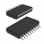 74LV245D,118
The activity of extra discounts on wholesale prices is in full swing…
Please fill in your contact information and we will send you the latest wholesale price list.





