 ChipApex | Global Electronic Components Supplier
74LVC07AD/AUJ
Search Product
Search Post
— IC芯片 | 连接器 | 传感器 | 被动器件 —
Search productSearch post
— IC芯片 | 连接器 | 传感器 | 被动器件 —
Consult the customer manager about the wholesale price.
consultation hotline:86-132-6715-2157
email:[email protected]
Contact the product manager for consultation. One-stop consultation is available.
Do you want a lower wholesale price? Please send us your inquiry and we will reply immediately.
The 74LVC07AD/AUJ is a hex buffer with open-drain outputs manufactured by Nexperia. It operates within a supply voltage range of 1.2 V to 5.5 V and features Schmitt-trigger inputs for tolerance against slow signal transitions. The device provides direct interface capability with TTL levels and includes overvoltage tolerant inputs up to 5.5 V. It complies with JEDEC standards for various voltage domains, including JESD8-7A, JESD8-5A, and JESD8-C/JESD36. ESD protection exceeds 2000 V (HBM) and 1000 V (CDM). Operating temperatures are specified from -40 °C to +85 °C and -40 °C to +125 °C.
Verify the specific package variant required, as the 74LVC07AD designation corresponds to the SO14 plastic small outline package (SOT108-1). Confirm that the application environment falls within the specified temperature ranges of -40 °C to +85 °C or -40 °C to +125 °C. Ensure supply voltage constraints remain within the 1.2 V to 5.5 V operational limits defined in the recommended operating conditions.
Select this component when an open-drain output topology is necessary for wired-AND configurations or level shifting. The wide supply voltage range supports operation across multiple logic families. Verify that the required package type matches the design footprint, specifically the SO14 form factor for the AD suffix. Consider the thermal dissipation requirements if operating near the upper temperature limits.
This part belongs to the 74LVC07A family of hex buffers produced by Nexperia. The 'AD' suffix identifies the specific SO14 package variant. The series utilizes CMOS technology optimized for low-voltage operation while maintaining compatibility with higher voltage interfaces. This family is designed for general-purpose digital buffering tasks in consumer and industrial electronics.
Direct substitutes include the SN74LVC07AD from Texas Instruments. Other compatible alternatives may include parts from Diodes Incorporated or onsemi, provided they match the open-drain output requirement and pinout configuration.
The open-drain outputs allow the device to interface directly with 5 V logic systems and support wired-AND connections, enabling use as translators in mixed voltage environments.
Schmitt-trigger action at all inputs makes the circuit tolerant of slower input rise and fall times, ensuring stable switching behavior.
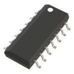 74LVC07AD/AUJ
The activity of extra discounts on wholesale prices is in full swing…
Please fill in your contact information and we will send you the latest wholesale price list.





