ChipApex | Global Electronic Components Supplier
74LVC07APW,112
Search Product
Search Post
— IC芯片 | 连接器 | 传感器 | 被动器件 —
Search productSearch post
— IC芯片 | 连接器 | 传感器 | 被动器件 —
Consult the customer manager about the wholesale price.
consultation hotline:86-132-6715-2157
email:[email protected]
Contact the product manager for consultation. One-stop consultation is available.
Do you want a lower wholesale price? Please send us your inquiry and we will reply immediately.
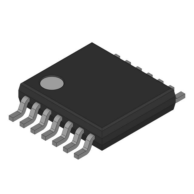
The Nexperia 74LVC07APW,112 is a hex buffer with open-drain outputs designed for mixed voltage environments. It operates within a supply voltage range of 1.2 V to 5.5 V and features Schmitt-trigger inputs for tolerance to slow rise and fall times. The device provides five-volt tolerant inputs and outputs, allowing direct interfacing with TTL levels. It complies with JEDEC standards JESD8-7A, JESD8-5A, and JESD8-C/JESD36. ESD protection exceeds 2000 V (HBM) and 1000 V (CDM). Operating temperatures are specified from -40 °C to +85 °C and up to +125 °C.
Verify the specific ordering suffix matches the required package type and temperature range. Confirm that the component meets the necessary JEDEC compliance standards for your application environment. Ensure that the supply voltage and input/output voltage levels remain within the recommended operating conditions defined in the datasheet to prevent damage or malfunction.
Select this component when a hex buffer with open-drain outputs is required for interfacing different voltage domains. The wide supply voltage range supports operation from low-power 1.2 V systems up to standard 5.5 V logic. Consider the TSSOP14 package dimensions if space constraints align with the SOT402-1 outline specifications provided in the documentation.
This part belongs to the 74LVC07A family of hex buffers with open-drain outputs manufactured by Nexperia. The APW suffix indicates the TSSOP14 plastic thin shrink small outline package (SOT402-1). The device is designed for CMOS low power consumption and direct interface with TTL levels, making it suitable for various general-purpose logic applications requiring robust input characteristics.
Direct substitutes include other 74LVC07 variants in compatible packages such as SO14 or DHVQFN14. Verify pinout compatibility and electrical specifications before substitution. Cross-reference with similar open-drain hex buffers from other manufacturers if package availability is limited.
The open-drain outputs allow the device to interface with 5 V logic systems even when powered by lower voltages, facilitating level translation in mixed voltage environments.
Schmitt-trigger action makes the circuit highly tolerant of slower input rise and fall times, ensuring reliable switching performance with noisy or gradual signals.
 74LVC07APW,112
The activity of extra discounts on wholesale prices is in full swing…
Please fill in your contact information and we will send you the latest wholesale price list.