 ChipApex | Global Electronic Components Supplier
SEARCH
Search Product
Search Post
— IC芯片 | 连接器 | 传感器 | 被动器件 —
Search productSearch post
— IC芯片 | 连接器 | 传感器 | 被动器件 —
Consult the customer manager about the wholesale price.
consultation hotline:86-132-6715-2157
email:[email protected]
Contact the product manager for consultation. One-stop consultation is available.
Do you want a lower wholesale price? Please send us your inquiry and we will reply immediately.
The 74LVC109DB,112 is a dual JK flip-flop from the NXP 74LVC series, housed in a 16-SSOP package. It operates on a supply voltage range of 1.65V to 3.6V with a quiescent current of 10 µA and input capacitance of 5 pF. The device supports set and reset functions with differential outputs and functions as a positive-edge-triggered JK type. It is rated for an operating temperature range of -40°C to 125°C (TA) and complies with RoHS3 standards.
Verify the specific ordering code suffix against official NXP documentation to ensure correct packaging and environmental compliance status. Confirm that the SSOP package variant matches the required footprint for PCB layout. Cross-reference the RoHS3 certification details with current regulatory requirements for the target market. Ensure the supply voltage specifications align with the system's power domain before integration.
Select this component when dual independent JK flip-flops are required within low-voltage CMOS logic families. The wide operating temperature range makes it suitable for industrial applications. Consider the differential output requirement and positive-edge trigger characteristic for timing-sensitive designs. Verify compatibility with existing 3.3V or lower logic levels in the circuit architecture.
This part belongs to the 74LVC logic family, designed for low-voltage operation between 1.65V and 3.6V. It serves as a digital storage element within complex integrated circuits, providing reliable state retention. The 74LVC series offers performance comparable to higher voltage logic while maintaining compatibility with modern low-power microcontrollers and processors.
Check for direct pin-compatible alternatives within the 74LVC series such as other dual JK flip-flop variants. Verify if the 74HC109 series is suitable if higher voltage tolerance is acceptable, noting potential differences in switching speed and drive capability.
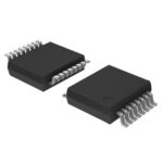 74LVC109DB,112
The activity of extra discounts on wholesale prices is in full swing…
Please fill in your contact information and we will send you the latest wholesale price list.





