 ChipApex | Global Electronic Components Supplier
74LVC125ADB,112
Search Product
Search Post
— IC芯片 | 连接器 | 传感器 | 被动器件 —
Search productSearch post
— IC芯片 | 连接器 | 传感器 | 被动器件 —
Consult the customer manager about the wholesale price.
consultation hotline:86-132-6715-2157
email:[email protected]
Contact the product manager for consultation. One-stop consultation is available.
Do you want a lower wholesale price? Please send us your inquiry and we will reply immediately.
The Nexperia 74LVC125ADB,112 is a quad buffer and line driver featuring 3-state outputs controlled by active LOW enable inputs (nOE). It operates within a supply voltage range of 1.2 V to 3.6 V and supports overvoltage tolerant inputs up to 5.5 V. The device includes IOFF circuitry for partial power-down applications. Propagation delay ranges from 1.0 ns to 12.8 ns depending on voltage. Output drive capability reaches ±24 mA at 3.0 V. It functions reliably across an ambient temperature range of -40 °C to +125 °C.
Verify the specific ordering suffix '112' against the manufacturer's latest documentation to confirm packaging details and tape/reel specifications. Ensure the SO14 package variant matches the required board layout constraints. Confirm compliance with RoHS directives and REACH regulations for the intended market before finalizing procurement orders.
Select this component when designing systems requiring level shifting between 3.3 V and 5 V logic families. The wide supply voltage range allows flexibility in low-power designs. The inclusion of Schmitt triggers makes it suitable for noisy environments or signals with slow transitions. Verify that the 3-state output configuration aligns with bus architecture requirements.
This part belongs to the 74LVC125A family of quad buffers with 3-state outputs. It is designed for high-speed digital applications requiring robust signal integrity. The device is specified for industrial temperature ranges and offers multiple package options including SO14, TSSOP14, and QFN variants for diverse PCB form factors.
Check for pin-compatible alternatives within the same LVC series if package availability is constrained. Ensure any substitute maintains the 5.5 V input tolerance and 3-state functionality. Verify that dynamic characteristics such as propagation delay meet the system timing requirements.
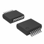 74LVC125ADB,112
The activity of extra discounts on wholesale prices is in full swing…
Please fill in your contact information and we will send you the latest wholesale price list.





