 ChipApex | Global Electronic Components Supplier
74LVC125ADB,118
Search Product
Search Post
— IC芯片 | 连接器 | 传感器 | 被动器件 —
Search productSearch post
— IC芯片 | 连接器 | 传感器 | 被动器件 —
Consult the customer manager about the wholesale price.
consultation hotline:86-132-6715-2157
email:[email protected]
Contact the product manager for consultation. One-stop consultation is available.
Do you want a lower wholesale price? Please send us your inquiry and we will reply immediately.
The Nexperia 74LVC125ADB,118 is a quad buffer/line driver with 3-state outputs controlled by active LOW output enable inputs (nOE). It features Schmitt-trigger inputs and IOFF circuitry for partial power-down protection. The device operates within a supply voltage range of 1.2 V to 3.6 V, supporting overvoltage tolerant inputs up to 5.5 V. It provides balanced propagation delays and direct interface capability with TTL levels. The component is specified for operation from -40 °C to +125 °C and complies with JEDEC standards JESD8-7A, JESD8-5A, and JESD8-C/JESD36.
Verify the specific ordering suffix 'ADB' against official Nexperia documentation, as it may indicate a distinct package or variant not explicitly detailed in the standard 74LVC125A datasheet. Confirm RoHS compliance and halogen-free status through manufacturer chemical content declarations. Ensure design-in validation includes checking absolute maximum ratings and thermal derating curves for the intended operating environment.
Select this component when designing systems requiring bidirectional level shifting or buffering between different voltage domains. The inclusion of IOFF circuitry makes it suitable for battery-powered applications where partial power-down modes are necessary to minimize leakage currents. Verify that the required output drive strength and propagation delay specifications align with the system's timing constraints.
This part belongs to the 74LVC125A family of low-voltage CMOS logic devices manufactured by Nexperia. The family offers multiple package options including SO14, TSSOP14, DHVQFN14, and DHXQFN14. These devices are designed for high-speed digital applications requiring robust noise immunity and compatibility with various logic families.
The 74LVC125AD,118 serves as a direct pin-compatible replacement within the same series. Other variants such as the 74LVC125APW, 74LVC125ABQ, and 74LVC125ABZ offer alternative package types while maintaining identical electrical characteristics.
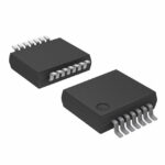 74LVC125ADB,118
The activity of extra discounts on wholesale prices is in full swing…
Please fill in your contact information and we will send you the latest wholesale price list.





