 ChipApex | Global Electronic Components Supplier
SEARCH
Search Product
Search Post
— IC芯片 | 连接器 | 传感器 | 被动器件 —
Search productSearch post
— IC芯片 | 连接器 | 传感器 | 被动器件 —
Consult the customer manager about the wholesale price.
consultation hotline:86-132-6715-2157
email:[email protected]
Contact the product manager for consultation. One-stop consultation is available.
Do you want a lower wholesale price? Please send us your inquiry and we will reply immediately.
The 74LVC1284D,118 is a 3.3V parallel printer interface transceiver and buffer designed for asynchronous, 4-bit bi-directional data transmission between personal computers and peripherals. It complies with IEEE 1284 standards (Level 1 & 2) and includes three additional lines for handshaking signals. The device features TTL-compatible inputs with at least 300mV hysteresis at VCC = 3.3V. It operates within a supply voltage range of 3.0V to 3.6V and supports an operating temperature range of 0°C to +70°C. The component is housed in a 20-pin plastic SO package.
Verify that the ordering code matches the specific package type required, as the 74LVC1284 family is available in multiple configurations including 20-pin plastic SO, SSOP Type II, and TSSOP Type I. Confirm the temperature range aligns with system requirements, noting that the standard D suffix indicates operation from 0°C to +70°C. Ensure compatibility with the target PCB footprint for the selected package variant before procurement.
Select this component when designing an asynchronous 4-bit parallel interface requiring IEEE 1284 compliance. It is suitable for applications needing TTL-compatible inputs and robust ESD protection. Consider the B-side output drive capabilities and the availability of high-drive enable options if stronger output currents are necessary. Verify that the 3.3V supply voltage range meets the system power architecture constraints.
The 74LVC1284 belongs to the LVC logic family, which is optimized for low-voltage operation. This specific part number represents the 20-pin plastic Small Outline (SO) package version. It serves as a specialized interface solution distinct from general-purpose bus drivers by integrating dedicated control lines for printer protocol handshaking directly into the transceiver structure.
Direct pin-to-pin replacements within the same package must maintain IEEE 1284 compliance and 4-bit bidirectional capability. Other variants such as 74LVC1284DB or 74LVC1284PW offer identical electrical functions but utilize different physical packages (SSOP or TSSOP). Cross-package substitution requires verifying mechanical fit and thermal characteristics.
The DC input voltage on the A side can range from -0.5V to VCC + 0.5V.
The HD pin enables or disables the high drive mode for the B/Y side outputs, allowing them to operate in either totem pole or open drain style depending on its state.
Yes, all inputs are TTL compatible and feature at least 300mV of input hysteresis at VCC = 3.3V.
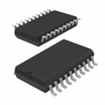 74LVC1284D,118
The activity of extra discounts on wholesale prices is in full swing…
Please fill in your contact information and we will send you the latest wholesale price list.







