 ChipApex | Global Electronic Components Supplier
74LVC1G125FS3-7
Search Product
Search Post
— IC芯片 | 连接器 | 传感器 | 被动器件 —
Search productSearch post
— IC芯片 | 连接器 | 传感器 | 被动器件 —
Consult the customer manager about the wholesale price.
consultation hotline:86-132-6715-2157
email:[email protected]
Contact the product manager for consultation. One-stop consultation is available.
Do you want a lower wholesale price? Please send us your inquiry and we will reply immediately.
The 74LVC1G125FS3-7 is a single non-inverting buffer and bus driver featuring a 3-state output, manufactured by Diodes Incorporated. It operates within a supply voltage range of 1.65V to 5.5V and provides an output drive capability of ±24mA at 3.3V. The device incorporates IOFF circuitry to support partial power-down applications by disabling the output and preventing damaging current backflow when powered down. Inputs are tolerant to 5.5V, enabling direct interface with TTL levels in mixed-voltage environments. It is housed in an X2-DFN0808-4 package.
Verify the specific FS3 suffix corresponds to the X2-DFN0808-4 package configuration before procurement. Confirm that the required operating temperature range aligns with the specified -40°C to +125°C limits. Ensure input signals remain within the absolute maximum ratings to prevent device failure. Check for compliance with RoHS and halogen-free requirements if environmental standards apply to the assembly process.
Select this component for designs requiring a compact single-channel buffer with controlled output impedance. The wide supply voltage range supports various low-power digital systems. The inclusion of partial power-down capabilities makes it suitable for battery-operated devices where leakage current management is critical. Verify that the package dimensions fit the available PCB real estate constraints.
This part belongs to the 74LVC1G125 series of single bus buffer gates with 3-state outputs produced by Diodes Incorporated. The FS3 ordering suffix specifically designates the X2-DFN0808-4 package variant. Other variants in the series utilize different packages such as SOT25 or SOT353, offering flexibility for diverse board layout requirements while maintaining identical logical functionality.
Direct substitutes include other 74LVC1G125 variants from Diodes Incorporated using different packages like SE (SOT353) or W5 (SOT25). Cross-manufacturer equivalents must be verified against the electrical characteristics and pinout definitions to ensure functional compatibility without redesigning the host circuit.
The device includes IOFF circuitry that automatically disables the output when the device is powered down. This prevents damaging current backflow from the output pins into the VCC rail.
The Output Enable (OE) pin controls the 3-state output. When a HIGH-level signal is applied to the OE pin, the output enters a high-impedance state, effectively disconnecting it from the circuit.
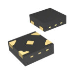 74LVC1G125FS3-7
The activity of extra discounts on wholesale prices is in full swing…
Please fill in your contact information and we will send you the latest wholesale price list.





