 ChipApex | Global Electronic Components Supplier
74LVC1G125GV/DG125
Search Product
Search Post
— IC芯片 | 连接器 | 传感器 | 被动器件 —
Search productSearch post
— IC芯片 | 连接器 | 传感器 | 被动器件 —
Consult the customer manager about the wholesale price.
consultation hotline:86-132-6715-2157
email:[email protected]
Contact the product manager for consultation. One-stop consultation is available.
Do you want a lower wholesale price? Please send us your inquiry and we will reply immediately.
The NXP USA Inc. 74LVC1G125GV/DG125 is a single non-inverting bus buffer and line driver featuring three-state outputs controlled by an OE input. It operates within a supply voltage range of 1.65 V to 5.5 V, supporting mixed 3.3 V and 5 V environments. The device includes Schmitt-trigger inputs for slow signal tolerance and IOFF circuitry for partial power-down protection. It provides high noise immunity, direct TTL interface capability, and robust ESD protection exceeding 2000 V (HBM).
Verify the specific package designation 'GV' corresponds to the SC-74A (SOT753) form factor as defined in the official ordering information table. Confirm that the suffix 'DG125' aligns with the manufacturer's standard packaging and marking codes. Ensure compatibility with the specified -40 °C to +125 °C temperature range for your operational environment.
Select this component when a single-channel non-inverting buffer with active-high enable control is required. It is suitable for designs needing Schmitt-trigger action on inputs to handle noisy or slow signals. The wide supply range makes it appropriate for interfacing between different logic families without level shifting components.
This part belongs to the Nexperia 74LVC family of low-voltage CMOS logic devices. The '1G' designation indicates a single functional element per package. The '125' series specifically denotes a non-inverting buffer with three-state outputs, distinguishing it from inverters or drivers with fixed outputs.
Consult the official datasheet section on similar parts for verified substitutes. Potential replacements include other 74LVC1G125 variants with different packages such as GW (TSSOP5), GM (XSON6), or GN (XSON6), provided the pinout and electrical characteristics remain compatible with the design.
The IOFF circuitry automatically disables the output when the device is powered down, preventing potentially damaging backflow current through the device if external voltages are present on the I/O pins.
The Schmitt-trigger action at all inputs makes the circuit tolerant of slower input rise and fall times, ensuring clean switching even with degraded signal edges.
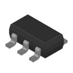 74LVC1G125GV/DG125
The activity of extra discounts on wholesale prices is in full swing…
Please fill in your contact information and we will send you the latest wholesale price list.





