 ChipApex | Global Electronic Components Supplier
74LVC1G126FW5-7
Search Product
Search Post
— IC芯片 | 连接器 | 传感器 | 被动器件 —
Search productSearch post
— IC芯片 | 连接器 | 传感器 | 被动器件 —
Consult the customer manager about the wholesale price.
consultation hotline:86-132-6715-2157
email:[email protected]
Contact the product manager for consultation. One-stop consultation is available.
Do you want a lower wholesale price? Please send us your inquiry and we will reply immediately.
The Diodes Incorporated 74LVC1G126FW5-7 is a single non-inverting buffer with a 3-state output, designed for operation within a power supply range of 1.65V to 5.5V. It features an X1-DFN1010-6 (Type B) package and operates across a temperature range of -40°C to +125°C. The device supports partial power-down applications via integrated IOFF circuitry, which disables outputs to prevent damaging current backflow when powered down. Inputs accept up to 5.5V, enabling direct interface with TTL levels in mixed-voltage environments.
Verify the specific FW5 ordering suffix corresponds to the X1-DFN1010-6 (Type B) package configuration before procurement. Confirm that the component meets RoHS 3 compliance requirements for your target market. Ensure design layouts adhere to the manufacturer's suggested pad dimensions for the X1-DFN1010-6 footprint to guarantee proper soldering and thermal performance.
Select this component when a single-channel non-inverting buffer with 3-state control is required for low-power CMOS applications. The wide operating voltage range allows compatibility with various system architectures. Consider the X1-DFN1010-6 package size constraints and verify that the thermal resistance characteristics meet the thermal management requirements of the final assembly environment.
This part belongs to the 74LVC1G126 series of single-buffer gates manufactured by Diodes Incorporated. The series utilizes LVC technology to provide robust performance across a broad voltage spectrum. The FW5 variant specifically denotes the X1-DFN1010-6 surface-mount package option, distinguishing it from other physical form factors available within the same logical family.
Cross-reference with other manufacturers offering the 74LVC1G126 specification to ensure pinout and electrical parameter compatibility. Verify that alternative packages maintain the same functional behavior regarding the OE input and IOFF state activation.
The IOFF circuitry automatically disables the output when the device is powered down, preventing damaging current from flowing back through the I/O pins into the disabled supply rail.
The inputs are tolerant to 5.5V, allowing the device to be used in mixed-voltage environments where input signals may exceed the VCC supply voltage.
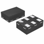 74LVC1G126FW5-7
The activity of extra discounts on wholesale prices is in full swing…
Please fill in your contact information and we will send you the latest wholesale price list.





