 ChipApex | Global Electronic Components Supplier
SEARCH
Search Product
Search Post
— IC芯片 | 连接器 | 传感器 | 被动器件 —
Search productSearch post
— IC芯片 | 连接器 | 传感器 | 被动器件 —
Consult the customer manager about the wholesale price.
consultation hotline:86-132-6715-2157
email:[email protected]
Contact the product manager for consultation. One-stop consultation is available.
Do you want a lower wholesale price? Please send us your inquiry and we will reply immediately.
The Nexperia 74LVC1G175GW,125 is a single D-type flip-flop with reset in a SOT-363 (6-TSSOP) package. It operates on a supply voltage of 1.65 V to 5.5 V. The device features positive-edge triggering and includes an asynchronous active LOW master reset input. Key electrical parameters include a maximum clock frequency of 200 MHz and a propagation delay of 4 ns at 5 V with 50 pF load. Output drive capability is ±32 mA, with static current of 10 µA. It supports partial power-down via I_OFF circuitry and withstands ESD up to 2000 V (HBM). Operating temperature ranges from -40 °C to +125 °C.
Verify the complete part number including the suffix ',125' to ensure correct tape-and-reel packaging configuration. Confirm that the SOT-363 package variant matches your PCB footprint requirements. Check for automotive grade variants if AEC-Q100 qualification is necessary for your specific application environment. Ensure compatibility with your system's voltage levels given the wide operating range.
Select this component when a single-bit storage element with asynchronous reset is required in space-constrained designs. The SOT-363 package offers a compact solution compared to standard TSSOP options. Consider the 200 MHz speed limit for high-frequency clocking applications. The I_OFF feature is critical for systems requiring power management during standby states. Verify input voltage compatibility if interfacing directly with 5 V logic sources.
This device belongs to the Nexperia 74LVC1G series, which focuses on single-gate miniaturized logic solutions. The LVC family is designed for low-voltage operation while maintaining compatibility with higher voltage interfaces. The 74LVC1G175 specifically addresses the need for simple sequential logic elements in modern portable and battery-powered devices where size and power consumption are primary constraints.
74LVC1G175GV,125 (SC-74A-5 package)
The master reset is asynchronous and active LOW, meaning it forces the output to a defined state regardless of the clock input status.
It disables the output drivers when the device is powered down, preventing damaging backflow currents from flowing through the device.
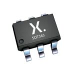 74LVC1G175GW,125
The activity of extra discounts on wholesale prices is in full swing…
Please fill in your contact information and we will send you the latest wholesale price list.





