 ChipApex | Global Electronic Components Supplier
SEARCH
Search Product
Search Post
— IC芯片 | 连接器 | 传感器 | 被动器件 —
Search productSearch post
— IC芯片 | 连接器 | 传感器 | 被动器件 —
Consult the customer manager about the wholesale price.
consultation hotline:86-132-6715-2157
email:[email protected]
Contact the product manager for consultation. One-stop consultation is available.
Do you want a lower wholesale price? Please send us your inquiry and we will reply immediately.
The Nexperia 74LVC1G74GT,115 is a single D-type edge-triggered flip-flop housed in an 8-XFDFN package. It operates within a supply voltage range of 1.65 V to 5.5 V and supports a maximum clock frequency of 200 MHz. The device features set and reset functions with complementary outputs capable of sourcing and sinking 32 mA. Propagation delay is specified at 4.1 ns under 5 V conditions with 50 pF load, while static current consumption is limited to 4 µA.
Verify the complete part number including the suffix to confirm the specific 8-XFDFN package configuration. Ensure compatibility with the target operating voltage range between 1.65 V and 5.5 V. Confirm that the required propagation delay and output drive current meet the system specifications before finalizing procurement decisions.
Select this component when a single-bit memory element with set and reset capabilities is required in a minimal footprint. The 8-XFDFN package offers space efficiency compared to larger alternatives. Consider the 200 MHz speed capability for high-frequency timing applications. Verify input capacitance and static current requirements against low-power design constraints.
This component belongs to the 74LVC family of low-voltage CMOS logic devices manufactured by Nexperia. The LVC series is designed for applications requiring operation at lower supply voltages while maintaining compatibility with standard logic levels. The 74LVC1G74 variant specifically provides a single D-type flip-flop function within a compact integrated circuit format suitable for modern portable electronics.
The device uses positive-edge triggering, meaning it captures the input data state on the rising edge of the clock signal.
Yes, the 74LVC1G74GT,115 includes both set (preset) and reset inputs that allow direct control of the output state independent of the clock signal.
The component features complementary outputs, providing both the non-inverted Q output and the inverted Q-bar output simultaneously.
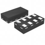 74LVC1G74GT,115
The activity of extra discounts on wholesale prices is in full swing…
Please fill in your contact information and we will send you the latest wholesale price list.





