 ChipApex | Global Electronic Components Supplier

SEARCH
Search Product
Search Post
— IC芯片 | 连接器 | 传感器 | 被动器件 —
Search productSearch post
— IC芯片 | 连接器 | 传感器 | 被动器件 —
Consult the customer manager about the wholesale price.
consultation hotline:86-132-6715-2157
email:[email protected]
Contact the product manager for consultation. One-stop consultation is available.
Do you want a lower wholesale price? Please send us your inquiry and we will reply immediately.
74LVC1G98GV-Q100H is listed in the Gates And Inverters - Multi-Function, Configurable range at ChipApex. The manufacturer field lists Nexperia USA Inc.. Its product description is 74LVC1G98GV-Q100/SOT457/SC-74. Review the specifications below when checking this part for your BOM.
The Nexperia 74LVC1G98GV-Q100H is a low-power configurable multiple function gate with Schmitt-trigger inputs, housed in an SC-74 (TSOP6) package. It supports a supply voltage range of 1.65 V to 5.5 V and operates within an ambient temperature range of -40 °C to +125 °C. The device features ±24 mA output drive capability at 3.0 V and includes IOFF circuitry for partial power-down applications. Propagation delay ranges from 5.1 ns to 18.0 ns depending on the supply voltage.
Verify the specific ordering suffix GV corresponds to the SC-74 TSOP6 package configuration required for your design. Confirm that the Q100 designation aligns with your automotive grade requirements. Ensure compatibility with the specified operating temperature range and supply voltage limits before finalizing procurement specifications.
Select this component when a single gate must perform multiple logic functions or act as a translator between different voltage domains. The inclusion of Schmitt triggers makes it suitable for noisy environments. Verify that the SC-74 package dimensions fit your PCB layout constraints and that the propagation delays meet your timing requirements across the full voltage range.
This part belongs to the 74LVC1G98-Q100 family of configurable gates. The GV suffix specifically denotes the SC-74 plastic surface-mounted package variant. It shares functional characteristics with other members of the LVC series but offers unique configurability through its three data inputs.
Check for 74LVC1G98GW-Q100H if a TSSOP6 package is acceptable instead of SC-74. Verify pinout compatibility and electrical specifications against any alternative configurable gates from other manufacturers.
The device can be configured as MUX, AND, OR, NAND, NOR, inverter, or buffer by connecting the three data inputs (A, B, C) to VCC or GND according to the function selection table.
The IOFF circuitry disables the output when the device is powered down, preventing damaging backflow current through the device in partial power-down applications.
Explore related parts through Logic, Integrated Circuits (ICs), all product categories, ChipApex homepage.
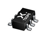 74LVC1G98GV-Q100H

The activity of extra discounts on wholesale prices is in full swing…
Please fill in your contact information and we will send you the latest wholesale price list.





