 ChipApex | Global Electronic Components Supplier
SEARCH
Search Product
Search Post
— IC芯片 | 连接器 | 传感器 | 被动器件 —
Search productSearch post
— IC芯片 | 连接器 | 传感器 | 被动器件 —
Consult the customer manager about the wholesale price.
consultation hotline:86-132-6715-2157
email:[email protected]
Contact the product manager for consultation. One-stop consultation is available.
Do you want a lower wholesale price? Please send us your inquiry and we will reply immediately.
The Nexperia 74LVC1T45GW,125 is a single-bit dual-supply translating transceiver with three-state outputs. It enables bidirectional level translation between two independent voltage domains, VCC(A) and VCC(B), both ranging from 1.2 V to 5.5 V. The device features a direction control input (DIR) that dictates data flow between port A and port B. It supports maximum data rates up to 420 Mbps for 3.3 V to 5.0 V translations. The component includes IOFF circuitry for partial power-down applications and operates within an ambient temperature range of -40 °C to +125 °C.
Verify the specific package variant against the required footprint, as the GW suffix denotes the TSSOP6 (SOT363-2) package. Confirm that the application requires the standard LVC functionality rather than the LVCH variant, which includes active bus hold circuitry for floating inputs. Ensure the design accommodates the specified operating temperature range and supply voltage limits for both ports.
Select this component when a single channel of bidirectional voltage translation is required between two distinct power domains. It is suitable for interfaces where the DIR pin can be actively controlled to manage data flow direction. Consider the LVCH version if the system requires internal bus holding to maintain valid logic levels on unused or floating inputs without external pull-up or pull-down resistors.
This device belongs to the 74LVC family of low-voltage CMOS logic components manufactured by Nexperia. It is specifically designed as a translating transceiver to bridge different voltage standards in modern electronic designs. The part is available in multiple package options, including XSON variants, but the GW suffix identifies the thin shrink small outline plastic package.
The 74LVCH1T45GW is a functional substitute within the same series, distinguished by the inclusion of active bus hold circuitry.
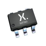 74LVC1T45GW,125
The activity of extra discounts on wholesale prices is in full swing…
Please fill in your contact information and we will send you the latest wholesale price list.





