 ChipApex | Global Electronic Components Supplier
74LVC241AD,118
Search Product
Search Post
— IC芯片 | 连接器 | 传感器 | 被动器件 —
Search productSearch post
— IC芯片 | 连接器 | 传感器 | 被动器件 —
Consult the customer manager about the wholesale price.
consultation hotline:86-132-6715-2157
email:[email protected]
Contact the product manager for consultation. One-stop consultation is available.
Do you want a lower wholesale price? Please send us your inquiry and we will reply immediately.
The 74LVC241AD,118 is an octal non-inverting buffer and line driver manufactured by Nexperia (formerly NXP) in the SO20 plastic small outline package. It operates within a supply voltage range of 1.2 V to 3.6 V and features Schmitt trigger inputs for improved noise immunity. The device provides 5 V tolerant inputs and outputs, allowing direct interfacing with 5 V logic systems while powered at lower voltages. It includes two independent output enable controls (1OE active LOW, 2OE active HIGH) managing high-impedance states.
Verify the manufacturer designation as Nexperia USA Inc., reflecting the corporate separation from NXP Semiconductors. Confirm the specific suffix 'AD' corresponds to the SO20 package variant with a -40 °C to +125 °C temperature range. Ensure compliance with RoHS standards and JEDEC specifications relevant to the target operating voltage.
Select this component when an octal buffer with 5 V tolerance is required for low-voltage CMOS applications. The SO20 package offers a wider body width compared to SSOP or TSSOP variants. Consider the specific enable pin polarities (active LOW for channel 1, active HIGH for channel 2) during schematic design to match system control logic.
This part belongs to the 74LVC family of low-voltage CMOS logic devices. It serves as a buffer solution for systems requiring level shifting between 1.2 V and 3.6 V supplies and 5 V external interfaces. The 'AD' suffix specifically identifies the SO20 package option within the broader 74LVC241A product line.
The datasheet lists 74LVC241ADB (SSOP20) and 74LVC241APW (TSSOP20) as alternative package options with identical electrical characteristics. No other functional substitutes are documented in the provided source material.
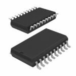 74LVC241AD,118
The activity of extra discounts on wholesale prices is in full swing…
Please fill in your contact information and we will send you the latest wholesale price list.





