 ChipApex | Global Electronic Components Supplier
74LVC2G126DP,125
Search Product
Search Post
— IC芯片 | 连接器 | 传感器 | 被动器件 —
Search productSearch post
— IC芯片 | 连接器 | 传感器 | 被动器件 —
Consult the customer manager about the wholesale price.
consultation hotline:86-132-6715-2157
email:[email protected]
Contact the product manager for consultation. One-stop consultation is available.
Do you want a lower wholesale price? Please send us your inquiry and we will reply immediately.
The Nexperia 74LVC2G126DP,125 is a dual bus buffer and line driver featuring three-state outputs controlled by active-high output enable inputs (nOE). It operates within a supply voltage range of 1.65 V to 5.5 V and accepts overvoltage tolerant inputs up to 5.5 V. The device incorporates Schmitt-trigger action for noise immunity and includes IOFF circuitry to prevent backflow current during partial power-down states. Packaged in an 8-lead TSSOP (SOT505-2) plastic thin shrink small outline package, it supports an ambient temperature range from -40 °C to +125 °C.
Verify the specific ordering suffix
Select this component for designs requiring dual-channel buffering with three-state control and robust noise immunity via Schmitt triggers. Ensure the application environment stays within the specified 1.65 V to 5.5 V supply range and -40 °C to +125 °C temperature limits. Confirm that the TSSOP8 package dimensions align with the PCB footprint requirements.
This part belongs to the 74LVC family of low-voltage CMOS logic devices manufactured by Nexperia. It is functionally equivalent to other variants in the 74LVC2G126 series, differing primarily in packaging options such as VSSOP or XSON. The DP suffix specifically denotes the TSSOP8 package configuration.
Direct replacements include other 74LVC2G126 variants with different packages, such as 74LVC2G126DC (VSSOP8), 74LVC2G126GT (XSON8), or 74LVC2G126GF (XSON8). Verify pin compatibility and thermal characteristics when substituting packages.
The IOFF circuitry automatically disables the outputs when the device is powered down (VCC = 0 V), preventing potentially damaging backflow current through the device from live input lines.
All inputs feature Schmitt-trigger action, which makes the circuit tolerant of slower input rise and fall times and provides high noise immunity.
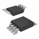 74LVC2G126DP,125
The activity of extra discounts on wholesale prices is in full swing…
Please fill in your contact information and we will send you the latest wholesale price list.





