 ChipApex | Global Electronic Components Supplier
74LVC2G126GD/S470,
Search Product
Search Post
— IC芯片 | 连接器 | 传感器 | 被动器件 —
Search productSearch post
— IC芯片 | 连接器 | 传感器 | 被动器件 —
Consult the customer manager about the wholesale price.
consultation hotline:86-132-6715-2157
email:[email protected]
Contact the product manager for consultation. One-stop consultation is available.
Do you want a lower wholesale price? Please send us your inquiry and we will reply immediately.
The Nexperia 74LVC2G126GD/S470 is a dual bus buffer and line driver featuring three-state outputs controlled by active-high output enable inputs (nOE). It operates within a supply voltage range of 1.65 V to 5.5 V and includes Schmitt-trigger inputs for noise immunity. The device incorporates IOFF circuitry to prevent backflow current during partial power-down states. Inputs are overvoltage tolerant up to 5.5 V, allowing direct interfacing with 3.3 V or 5 V devices in mixed-voltage environments.
Verify the specific package variant corresponding to the GD suffix against the manufacturer's ordering information table. Confirm that the S470 suffix aligns with the required marking code and reel specifications for your manufacturing process. Ensure compatibility with the specified temperature range and JEDEC standards before finalizing procurement orders.
Select this component when a dual buffer with three-state control and partial power-down protection is required. It is suitable for designs needing Schmitt-trigger inputs to handle slower signal transitions. Verify that the operating voltage range and output drive capabilities meet the system requirements for both low and high logic levels across the intended temperature spectrum.
This part belongs to the 74LVC2G126 family of dual bus buffers. The GD suffix typically denotes an XSON8 package variant. The series is designed for low power consumption and high noise immunity, complying with various JEDEC standards for different supply voltage ranges. It serves as a standard interface solution for digital logic systems requiring bidirectional or unidirectional buffering.
Direct replacements include other 74LVC2G126 variants with compatible packages such as GT, GF, GN, or GS. Ensure the substitute maintains the same pinout and electrical characteristics, particularly the IOFF functionality and Schmitt-trigger inputs, to guarantee functional equivalence in existing designs.
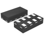 74LVC2G126GD/S470,
The activity of extra discounts on wholesale prices is in full swing…
Please fill in your contact information and we will send you the latest wholesale price list.





