 ChipApex | Global Electronic Components Supplier
74LVC2G17GW-Q100H
Search Product
Search Post
— IC芯片 | 连接器 | 传感器 | 被动器件 —
Search productSearch post
— IC芯片 | 连接器 | 传感器 | 被动器件 —
Consult the customer manager about the wholesale price.
consultation hotline:86-132-6715-2157
email:[email protected]
Contact the product manager for consultation. One-stop consultation is available.
Do you want a lower wholesale price? Please send us your inquiry and we will reply immediately.
The Nexperia 74LVC2G17GW-Q100H is a dual non-inverting Schmitt trigger buffer with 5 V tolerant inputs, designed for automotive applications. It operates within a supply voltage range of 1.65 V to 5.5 V and supports an ambient temperature range from -40 °C to +125 °C. The device features IOFF circuitry for partial power-down mode operation, preventing backflow current. It provides high noise immunity and direct interface with TTL levels. Propagation delay ranges from 1.0 ns to 13.1 ns depending on voltage and temperature. ESD protection exceeds 2000 V (HBM) and 1000 V (CDM).
Verify the specific package variant during procurement, as the GW suffix denotes the TSSOP6 (SOT363-2) package. Confirm that the required operating temperature range aligns with the specified -40 °C to +125 °C limits. Ensure design compatibility with the AEC-Q100 Grade 1 qualification if used in automotive contexts. Check for any recent Product Change Notifications regarding marking or packaging updates.
Select this component when dual-channel buffering with hysteresis is required in space-constrained designs. The 5 V tolerance feature makes it suitable for bridging different voltage domains without additional level shifters. Consider the propagation delay specifications relative to system timing requirements across the full operating voltage and temperature range. Verify input leakage characteristics if low power consumption is critical during standby modes.
This part belongs to the Nexperia 74LVC-Q100 family of automotive-grade logic ICs. The series offers various logic functions optimized for low power and high reliability in harsh environments. The 'Q100' designation indicates adherence to strict automotive quality standards, ensuring performance stability over extended temperature ranges and long operational lifetimes typical in vehicle electronics.
Direct replacements include other 74LVC2G17 variants from Nexperia, such as the GV version in SC-74/TSOP6 package. Cross-vendor equivalents must match the dual Schmitt trigger function, 5 V tolerance, and AEC-Q100 qualification. Verify pinout compatibility and electrical parameters before substitution.
The IOFF circuitry disables the outputs when the device is powered down, preventing potentially damaging backflow current through the device when connected to live buses.
The inputs are 5 V tolerant, allowing them to be driven from either 3.3 V or 5 V devices safely.
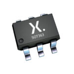 74LVC2G17GW-Q100H
The activity of extra discounts on wholesale prices is in full swing…
Please fill in your contact information and we will send you the latest wholesale price list.





