 ChipApex | Global Electronic Components Supplier
74LVC2G17GW,125
Search Product
Search Post
— IC芯片 | 连接器 | 传感器 | 被动器件 —
Search productSearch post
— IC芯片 | 连接器 | 传感器 | 被动器件 —
Consult the customer manager about the wholesale price.
consultation hotline:86-132-6715-2157
email:[email protected]
Contact the product manager for consultation. One-stop consultation is available.
Do you want a lower wholesale price? Please send us your inquiry and we will reply immediately.
The Nexperia 74LVC2G17GW,125 is a dual non-inverting Schmitt trigger buffer housed in a TSSOP6 (SOT363-2) package. It operates within a supply voltage range of 1.65 V to 5.5 V and features overvoltage tolerant inputs up to 5.5 V. The device provides high noise immunity and supports partial power-down mode via IOFF circuitry. Propagation delay ranges from 1.0 ns to 8.5 ns depending on voltage and temperature. It complies with JEDEC standards for various voltage levels and offers ESD protection exceeding 2000 V (HBM).
Verify the specific ordering suffix '125' against the manufacturer's latest documentation to confirm packaging details such as reel size or tape specifications. Ensure the TSSOP6 package variant matches the required PCB footprint dimensions. Confirm compliance requirements including RoHS status and halogen-free definitions prior to final procurement authorization.
Select this component when dual buffering with hysteresis is required in space-constrained designs. The TSSOP6 package is suitable for surface-mount applications requiring thin profiles. Consider the wide operating temperature range and low static power consumption for portable or industrial systems. Verify that the input voltage tolerance aligns with the source driver levels.
This part belongs to the 74LVC family of CMOS logic devices, designed for low-voltage operation. The 74LVC2G17 series specifically provides dual Schmitt trigger functionality. The GW suffix denotes the TSSOP6 plastic thin shrink small outline package. It is manufactured by Nexperia USA Inc. and is intended for general-purpose digital signal conditioning.
Check for equivalent parts within the same 74LVC family offering identical pinouts and electrical characteristics. Verify package compatibility if substituting with variants like the GV (SC-74) version. Ensure any replacement maintains the required Schmitt trigger action and IOFF functionality for partial power-down support.
The IOFF circuitry disables the outputs when the device is powered down, preventing potentially damaging backflow current through the device even if inputs are at 5.5 V while VCC is 0 V.
The inputs are overvoltage tolerant up to 5.5 V, allowing them to be driven by 3.3 V or 5 V devices without damage.
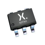 74LVC2G17GW,125
The activity of extra discounts on wholesale prices is in full swing…
Please fill in your contact information and we will send you the latest wholesale price list.





