 ChipApex | Global Electronic Components Supplier
74LVC2G240GD,125
Search Product
Search Post
— IC芯片 | 连接器 | 传感器 | 被动器件 —
Search productSearch post
— IC芯片 | 连接器 | 传感器 | 被动器件 —
Consult the customer manager about the wholesale price.
consultation hotline:86-132-6715-2157
email:[email protected]
Contact the product manager for consultation. One-stop consultation is available.
Do you want a lower wholesale price? Please send us your inquiry and we will reply immediately.
The Nexperia 74LVC2G240GD,125 is a dual inverting buffer and line driver featuring three-state outputs controlled by active-low enable inputs (1OE, 2OE). It operates within a supply voltage range of 1.65 V to 5.5 V and supports input voltages up to 5 V, enabling direct interfacing with TTL levels and mixed 3.3 V/5 V environments. The device incorporates Schmitt trigger inputs for noise immunity and IOFF circuitry to prevent backflow current during partial power-down states.
Verify the specific package designation against official documentation, as the 'GD' suffix does not appear in the standard ordering table for this series. Confirm the exact physical dimensions and lead configuration required for your PCB layout before finalizing procurement to avoid compatibility issues.
Select this component when designing systems requiring bidirectional or unidirectional buffering with defined high-impedance states. Ensure the application environment remains within the specified -40 °C to +125 °C temperature range and that input transition rates comply with JEDEC standards for the chosen supply voltage.
This part belongs to the 74LVC family of low-voltage CMOS logic devices manufactured by Nexperia. The family is characterized by wide supply voltage operation and compatibility with standard logic interfaces. This specific model provides dual buffering functionality within a compact integrated circuit form factor.
Publicly confirmed substitute part numbers are not available in the provided source material. Verify pinout compatibility and electrical specifications carefully if considering alternative manufacturers.
The three-state outputs are controlled by active-low enable inputs (1OE and 2OE). A HIGH level on these pins forces the outputs into a high-impedance OFF-state.
The IOFF circuitry disables the output to prevent potentially damaging backflow current through the device when it is in a powered-down state.
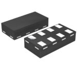 74LVC2G240GD,125
The activity of extra discounts on wholesale prices is in full swing…
Please fill in your contact information and we will send you the latest wholesale price list.





