 ChipApex | Global Electronic Components Supplier
SEARCH
Search Product
Search Post
— IC芯片 | 连接器 | 传感器 | 被动器件 —
Search productSearch post
— IC芯片 | 连接器 | 传感器 | 被动器件 —
Consult the customer manager about the wholesale price.
consultation hotline:86-132-6715-2157
email:[email protected]
Contact the product manager for consultation. One-stop consultation is available.
Do you want a lower wholesale price? Please send us your inquiry and we will reply immediately.
The Nexperia 74LVC2G74DP-Q100H is a dual D-type flip-flop with separate clock inputs, housed in an SOT505 (TSSOP8) package. It operates within a supply voltage range of 1.65 V to 5.5 V and supports data rates up to 333 MHz. The device features Schmitt-trigger inputs for noise tolerance and includes I_OFF circuitry for partial power-down protection. It complies with AEC-Q100 standards for automotive applications and offers ESD protection exceeding 2000 V (HBM).
Verify the specific suffix 'Q100H' against official Nexperia documentation to confirm AEC-Q100 qualification status and tape-and-reel packaging specifications. Ensure compatibility with target PCB footprint SOT505/TSSOP-8 dimensions. Cross-reference RoHS and REACH compliance declarations for regional regulatory adherence before finalizing procurement orders.
Select this component when dual independent D-flip-flops are required in space-constrained automotive designs. The wide supply voltage range facilitates interfacing across different logic levels. Verify that the operating temperature range meets system requirements and that the package size aligns with available board real estate constraints.
This part belongs to the Nexperia 74LVC family of low-voltage CMOS logic devices. The Q100 designation indicates automotive-grade qualification under AEC-Q100 standards. The DP suffix specifies the TSSOP8 surface-mount package. It provides robust performance for high-speed digital logic applications requiring reliable state retention.
Check Nexperia datasheets for alternative packages such as 74LVC2G74DC-Q100H or non-automated variants like 74LVC2G74DP,125 if automotive qualification is not strictly required. Ensure pinout compatibility and electrical parameter alignment before substitution.
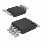 74LVC2G74DP-Q100H
The activity of extra discounts on wholesale prices is in full swing…
Please fill in your contact information and we will send you the latest wholesale price list.






