 ChipApex | Global Electronic Components Supplier

SEARCH
Search Product
Search Post
— IC芯片 | 连接器 | 传感器 | 被动器件 —
Search productSearch post
— IC芯片 | 连接器 | 传感器 | 被动器件 —
Consult the customer manager about the wholesale price.
consultation hotline:86-132-6715-2157
email:[email protected]
Contact the product manager for consultation. One-stop consultation is available.
Do you want a lower wholesale price? Please send us your inquiry and we will reply immediately.
74LVC4066D,112 is listed in the Analog Switches, Multiplexers, Demultiplexers range at ChipApex. The manufacturer field lists Nexperia USA Inc.. Its product description is IC SWITCH SPST-NO X 4 10OHM 14SO. Review the specifications below when checking this part for your BOM.
The Nexperia 74LVC4066D,112 is a high-speed Si-gate CMOS quad bilateral analog switch housed in an SO14 (SOT108-1) plastic small outline package. It provides four independent single-pole, single-throw switches with active HIGH enable inputs and Schmitt-trigger action for noise immunity. The device operates across a wide supply voltage range of 1.65 V to 5.5 V. Key electrical parameters include a typical ON resistance of 6.5 Ω at 3.3 V and 6 Ω at 5 V, with a maximum switch current capability of 32 mA. Propagation delay ranges from 0.2 ns to 2.0 ns depending on the supply voltage. ESD protection exceeds 2000 V (HBM) and 1000 V (CDM).
Verify the ordering suffix '112' against official Nexperia documentation to confirm tape-and-reel packaging specifications. Ensure the selected component matches the required temperature grade (-40 °C to +125 °C) and package variant (SO14/SOT108-1). Cross-reference the 12NC code 934066868115 for accurate procurement details.
Select this component when a quad bilateral switch with low ON resistance and wide voltage compatibility is required. Consider the SO14 package dimensions if board space allows for through-hole or standard surface-mount assembly. Evaluate the 32 mA switch current limit against load requirements to ensure reliable operation without exceeding thermal dissipation limits.
The 74LVC4066 belongs to the LVC (Low-Voltage CMOS) family, designed for high-speed applications requiring low power consumption. It serves as a direct replacement for older 4066 series devices while offering improved performance metrics such as lower ON resistance and higher ESD tolerance. The D suffix specifically denotes the SO14 plastic small outline package variant.
Direct pin-compatible replacements within the same family include the 74LVC4066PW (TSSOP14), 74LVC4066BQ (DHVQFN14), and 74LVC4066BZ (DHXQFN14). Verify that alternative packages meet the specific thermal and mechanical constraints of the target design.
The enable input (nE) controls the state of the switch. When nE is HIGH, the switch is turned ON, allowing signal flow between the Y and Z terminals. When nE is LOW, the switch is turned OFF, isolating the terminals.
The 74LVC4066 incorporates Schmitt-trigger action at the enable inputs. This feature makes the circuit tolerant of slower input rise and fall times across the entire operating voltage range from 1.65 V to 5.5 V.
The device offers ESD protection exceeding 2000 V according to the Human Body Model (HBM: ANSI/ESDA/JEDEC JS-001 class 2) and exceeding 1000 V according to the Charged Device Model (CDM: ANSI/ESDA/JEDEC JS-002 class C3).
Explore related parts through Interface, Integrated Circuits (ICs), all product categories, ChipApex homepage.
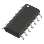 74LVC4066D,112

The activity of extra discounts on wholesale prices is in full swing…
Please fill in your contact information and we will send you the latest wholesale price list.





