 ChipApex | Global Electronic Components Supplier
74LVC541ADTR2G
Search Product
Search Post
— IC芯片 | 连接器 | 传感器 | 被动器件 —
Search productSearch post
— IC芯片 | 连接器 | 传感器 | 被动器件 —
Consult the customer manager about the wholesale price.
consultation hotline:86-132-6715-2157
email:[email protected]
Contact the product manager for consultation. One-stop consultation is available.
Do you want a lower wholesale price? Please send us your inquiry and we will reply immediately.
The MC74LVC541ADTR2G is an octal buffer and line driver manufactured by onsemi, belonging to the LVC logic family. It features non-inverting outputs with three-state capability controlled by two output enable inputs. The device operates within a supply voltage range of 1.2 V to 3.6 V and utilizes a 20-pin TSSOP surface-mount package. Key electrical specifications include a propagation delay of 8 ns at 3.3 V and 6 ns at 5 V, with high-level and low-level output currents of -24 mA and 24 mA respectively. Static current is specified at 8 uA, and the maximum power dissipation is 200 mW.
Verify the specific ordering suffix against the manufacturer's official documentation to confirm package type and tape-and-reel specifications. Ensure the component meets RoHS compliance requirements for your target market. Cross-reference the full part number with the latest datasheet revision to validate pinout compatibility and electrical characteristics before integration into production designs.
Select this component when designing circuits requiring octal buffering with three-state outputs in low-voltage environments. It is suitable for applications needing signal translation between different voltage levels due to its input tolerance. Consider the TSSOP-20 package constraints and thermal dissipation limits when evaluating board layout and operating temperature ranges.
This component is part of the MC74LVC541 series, which represents onsemi's Low Voltage CMOS technology. The series is designed for high-speed operations while maintaining low power consumption. The 'DTR2G' suffix indicates a specific tape-and-reel packaging configuration in a TSSOP-20 case, optimized for automated surface-mount assembly processes.
Compatible substitutes include the MC74AC541DTR2G for higher speed performance and the MC74HCT541ADTR2G for 5 V logic compatibility. Verify that alternative parts maintain the same 20-TSSOP footprint and three-state functionality to ensure direct pin-to-pin interchangeability without circuit redesign.
All inputs support Schmitt trigger action and can be driven from either 3.3 V or 5 V devices, enabling use as a translator in mixed-voltage environments.
Two output enable inputs (OE1 and OE2) control the state; when either is high, all outputs assume a high-impedance OFF-state.
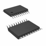 74LVC541ADTR2G
The activity of extra discounts on wholesale prices is in full swing…
Please fill in your contact information and we will send you the latest wholesale price list.





