 ChipApex | Global Electronic Components Supplier
74LVC541APW/AUJ
Search Product
Search Post
— IC芯片 | 连接器 | 传感器 | 被动器件 —
Search productSearch post
— IC芯片 | 连接器 | 传感器 | 被动器件 —
Consult the customer manager about the wholesale price.
consultation hotline:86-132-6715-2157
email:[email protected]
Contact the product manager for consultation. One-stop consultation is available.
Do you want a lower wholesale price? Please send us your inquiry and we will reply immediately.
The Nexperia 74LVC541A is an octal buffer and line driver featuring three-state outputs. It operates within a supply voltage range of 1.2 V to 3.6 V and supports overvoltage tolerant inputs up to 5.5 V, enabling direct interfacing with 5 V logic in mixed-voltage environments. The device includes IOFF circuitry for partial power-down applications to prevent backflow current. Inputs utilize Schmitt-trigger action to tolerate slower rise and fall times. It complies with JEDEC standards JESD8-7A, JESD8-5A, and JESD8-C/JESD36.
Verify the specific package variant against the ordering information table, such as TSSOP20 (SOT360-1), SO20 (SOT163-1), or DHVQFN20 (SOT764-1). Confirm the temperature range specification matches the application requirements, as the device is specified from -40 °C to +85 °C and -40 °C to +125 °C. Ensure compatibility with the required JEDEC standard version.
Select this component when an octal buffer with three-state capability is required for bus driving applications. The wide supply voltage range and 5 V tolerance make it suitable for bridging low-voltage logic with 5 V legacy systems. Consider the IOFF feature if the design involves partial power-down states to protect downstream components from reverse current flow.
This part belongs to the 74LVC541A family of octal buffers and line drivers manufactured by Nexperia. It is designed as a high-performance, low-power CMOS device compatible with advanced CMOS families. The product data sheet defines its electrical characteristics, pin configurations, and functional behavior for integration into digital logic circuits requiring bus isolation and level shifting.
Public confirmed substitute part numbers include 74LVC541AD and 74LVC541ABQ.
The device utilizes IOFF circuitry which disables the outputs when powered down, preventing potentially damaging backflow current through the device.
OE1 and OE2 are output enable inputs that are active LOW. A HIGH level on either pin causes the associated outputs to assume a high-impedance OFF-state.
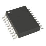 74LVC541APW/AUJ
The activity of extra discounts on wholesale prices is in full swing…
Please fill in your contact information and we will send you the latest wholesale price list.





