ChipApex | Global Electronic Components Supplier
74LVC541AQ20-13
Search Product
Search Post
— IC芯片 | 连接器 | 传感器 | 被动器件 —
Search productSearch post
— IC芯片 | 连接器 | 传感器 | 被动器件 —
Consult the customer manager about the wholesale price.
consultation hotline:86-132-6715-2157
email:[email protected]
Contact the product manager for consultation. One-stop consultation is available.
Do you want a lower wholesale price? Please send us your inquiry and we will reply immediately.
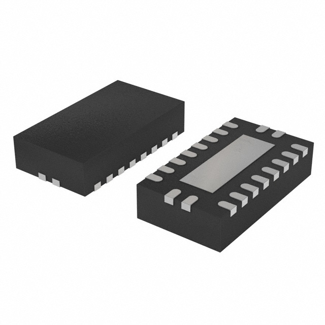
The Diodes Incorporated 74LVC541AQ20-13 is an octal buffer and line driver featuring three-state outputs, designed for driving bus lines or buffering memory address registers. It operates within a supply voltage range of 1.65V to 3.6V and supports mixed-voltage environments with inputs tolerant up to 5.5V. The device incorporates Schmitt trigger action at all inputs and includes I_OFF circuitry to prevent damaging current backflow during partial power-down conditions. Packaged in a V-QFN4525-20 format, it provides robust ESD protection exceeding 2000-V Human Body Model standards.
Verify the package code Q20 corresponds to the V-QFN4525-20 form factor before integration. Confirm the -13 suffix indicates 13-inch tape and reel packaging containing 2500 units per reel. Ensure design compatibility with the specified operating temperature range of -40°C to +125°C. Validate that the 5.5V input tolerance aligns with the target system's voltage levels to ensure proper functionality.
Select this component when an octal buffer with three-state capability is required for bus architectures. The V-QFN4525-20 package offers a compact footprint suitable for space-constrained designs. Consider the 5.5V input tolerance if interfacing with legacy 5V logic while operating from lower supply voltages. The inclusion of Schmitt triggers makes it suitable for noisy environments requiring clean signal transitions.
This part belongs to the 74LVC541A series of octal buffers and line drivers manufactured by Diodes Incorporated. The 'Q20' designation specifically identifies the V-QFN4525-20 surface-mount package variant, distinguishing it from other package options like TSSOP-20. The '-13' suffix denotes the standard 13-inch tape and reel packing configuration used for automated assembly processes.
Cross-reference pinouts and electrical characteristics with alternative octal buffer devices. Verify that substitute components support the same 1.65V to 3.6V supply range and 5.5V input tolerance. Ensure replacement parts offer comparable ESD protection levels and I_OFF functionality for partial power-down scenarios.
The device features I_OFF circuitry that disables the outputs when powered down, preventing damaging current backflow through the device.
OE1 and OE2 are active-low output enable inputs. If either input is high, all eight outputs enter a high-impedance state; data transfers from inputs to outputs only when both are low.
Yes, the inputs are tolerant to 5.5V, allowing the device to be used in mixed voltage environments where it interfaces with both 3.3V and 5V devices.
 74LVC541AQ20-13
The activity of extra discounts on wholesale prices is in full swing…
Please fill in your contact information and we will send you the latest wholesale price list.